

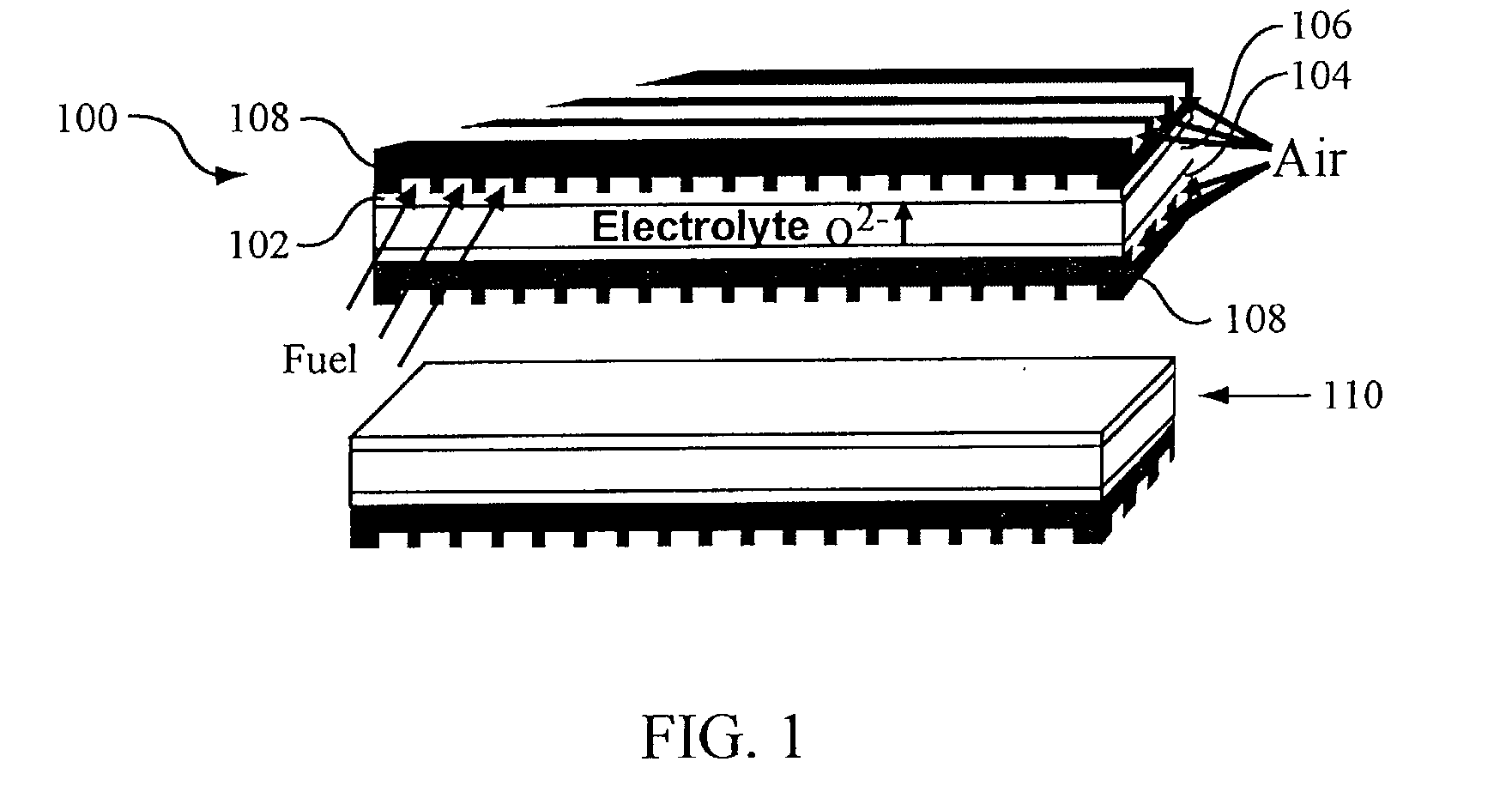
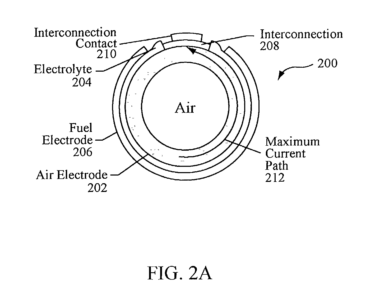
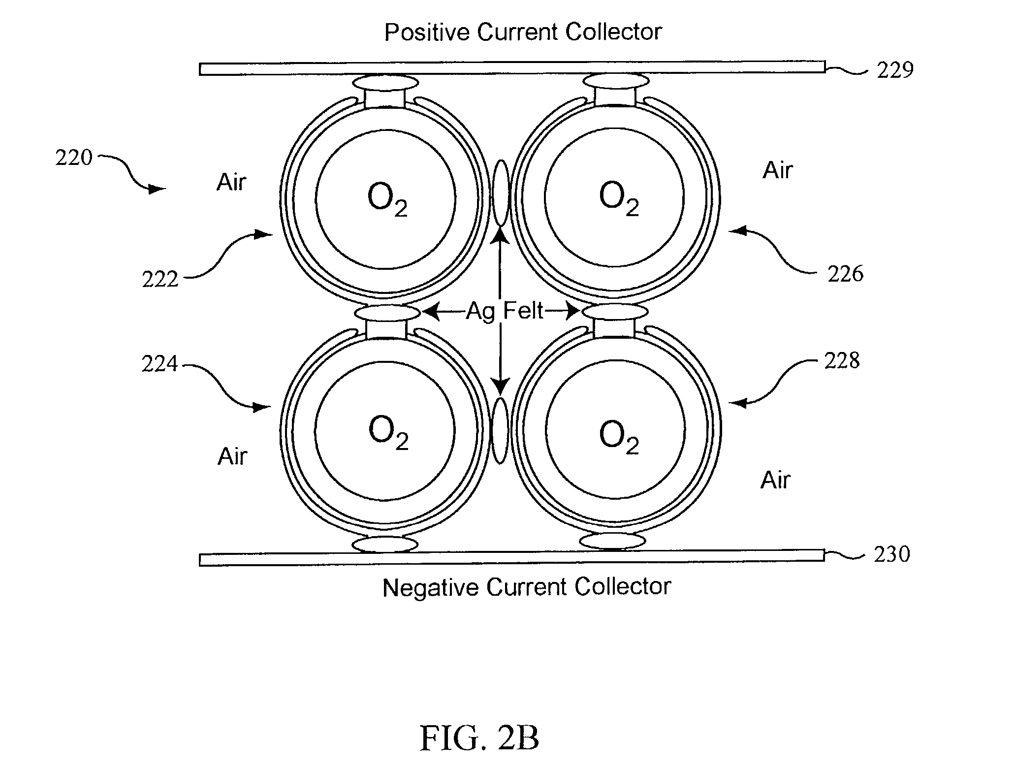
Structures and fabrication techniques for solid state electrochemical devices
a technology of electrochemical devices and structures, applied in the direction of sustainable manufacturing/processing, cell components, separation processes, etc., can solve the problems of high electrical resistance, high cost of manufacture, and inherently high electrical resistance of ceramic materials used in conventional solid-state electrochemical device implementations. achieve high electronic conductivity, reduce resistive losses in the device, and high strength
- Summary
- Abstract
- Description
- Claims
- Application Information
AI Technical Summary
Benefits of technology
Problems solved by technology
Method used
Image

Examples
example 1
Co-firing of YSZ Film on Inconel-Alumina Substrate
[0078]50 vol % Al2O3 (AKP-30) and 50 vol % Inconel 600 (Powder Alloy Corp.) with a small amount of binder (XUS 40303 from Dow Chemical Company) were mixed in water and dried. The resulting powder was ground in a mortar and pestle and sieved to <100 μm. 5 g of the powder was pressed to 5000 psi in an 1.5 in steel die. A thin layer of YSZ powder (Tosoh Corp.) was applied to one surface of the pressed disk. The coated disk was again pressed to 6000 psito increase the green density of the YSZ film and enhance adhesion. The disk was placed film side down in a molybdenum furnace under 2 psi flowing He. The furnace was manually heated to 450° C., and then at a rate of 5° C. / min to 1350° C., held for 4 hr, and then cooled at a rate of 5° C. / min. The resulting bilayer shrank 10%. The film side was shiny and clear, the uncoated side was slightly pinkish (chromia scale). FIGS. 6A and 6B show a scanning electron microscope (SEM) edge view of the...
PUM
| Property | Measurement | Unit |
|---|---|---|
| thick | aaaaa | aaaaa |
| thick | aaaaa | aaaaa |
| thick | aaaaa | aaaaa |
Abstract
Description
Claims
Application Information