Pressure-welded semiconductor device

a semiconductor device and pressure welding technology, applied in the direction of emergency protective circuit arrangement, nanostructure manufacturing, electrical apparatus construction details, etc., can solve the problems of insufficient performance of pressure-welded semiconductor devices, difficult diffusion of heat generated in semiconductor elements, and large electrical resistance between element-side electrodes and casing-side electrodes

Inactive Publication Date: 2006-01-17
TOYOTA CENT RES & DEV LAB INC
View PDF10 Cites 13 Cited by
  • Summary
  • Abstract
  • Description
  • Claims
  • Application Information

AI Technical Summary

Benefits of technology

[0013]It is an object of the present invention to solve the above-described problem. That is, it is an object of the invention to provide a pressure-welded semiconductor device in which electrical resistance and thermal resistance at pressure-welded portions between element-side electrodes and casing-side electrodes are small, even when a pressurizing force applied to a semiconductor element is small.
[0014]It is also an object of the invention to provide a pressure-welded semiconductor device whose mechanical reliability is high and whose electrical conductivity and thermal conductivity are high.

Problems solved by technology

When the real contact area is small, electrical resistance between the element-side electrodes and the casing-side electrodes becomes large and diffusion of heat generated in the semiconductor element becomes difficult.
In this case, the pressure-welded semiconductor device becomes unable to exhibit sufficient performance as a pressure-welded semiconductor device and reliability drops.
However, when the pressurizing force is increased, it is difficult to miniaturize and reduce the weight of the pressure-welded semiconductor device, and manufacturing costs also become high, because the configuration of pressurized portions for pressurization becomes large.
However, because a conductive nonwoven fabric is used, electricity and heat are transmitted only at contact points between the fibers, and the spaces between the fibers do not function as good conductors of electricity and heat.
Thus, when the technology described in JP-A No. 2000-68297 is compared with the case where a bulk conductive substance is disposed between the element-side electrodes and the casing-side electrodes by metal solder connection or the like, it is inferior in terms of the drop in electrical resistance and improving thermal conductivity.
In this case, the pressure-welded semiconductor device becomes unable to exhibit its original performance as a pressure-welded semiconductor element, and cases where problems such as the device electrically short-circuiting are possible.
This problem occurs not only when the conductive nonwoven fabric is positionally displaced, but there is also the potential for this problem to occur due to a drop in fibers of a long fiber length resulting from deterioration over time.
Moreover, because it becomes necessary to prevent positional displacement itself of the conductive nonwoven fabric at the time of manufacturing the pressure-welded semiconductor device, the assembly steps of the pressure-welded semiconductor device become more complicated and manufacturing costs also increase.

Method used


Image

  • Pressure-welded semiconductor device
  • Pressure-welded semiconductor device
  • Pressure-welded semiconductor device

Examples


example 1

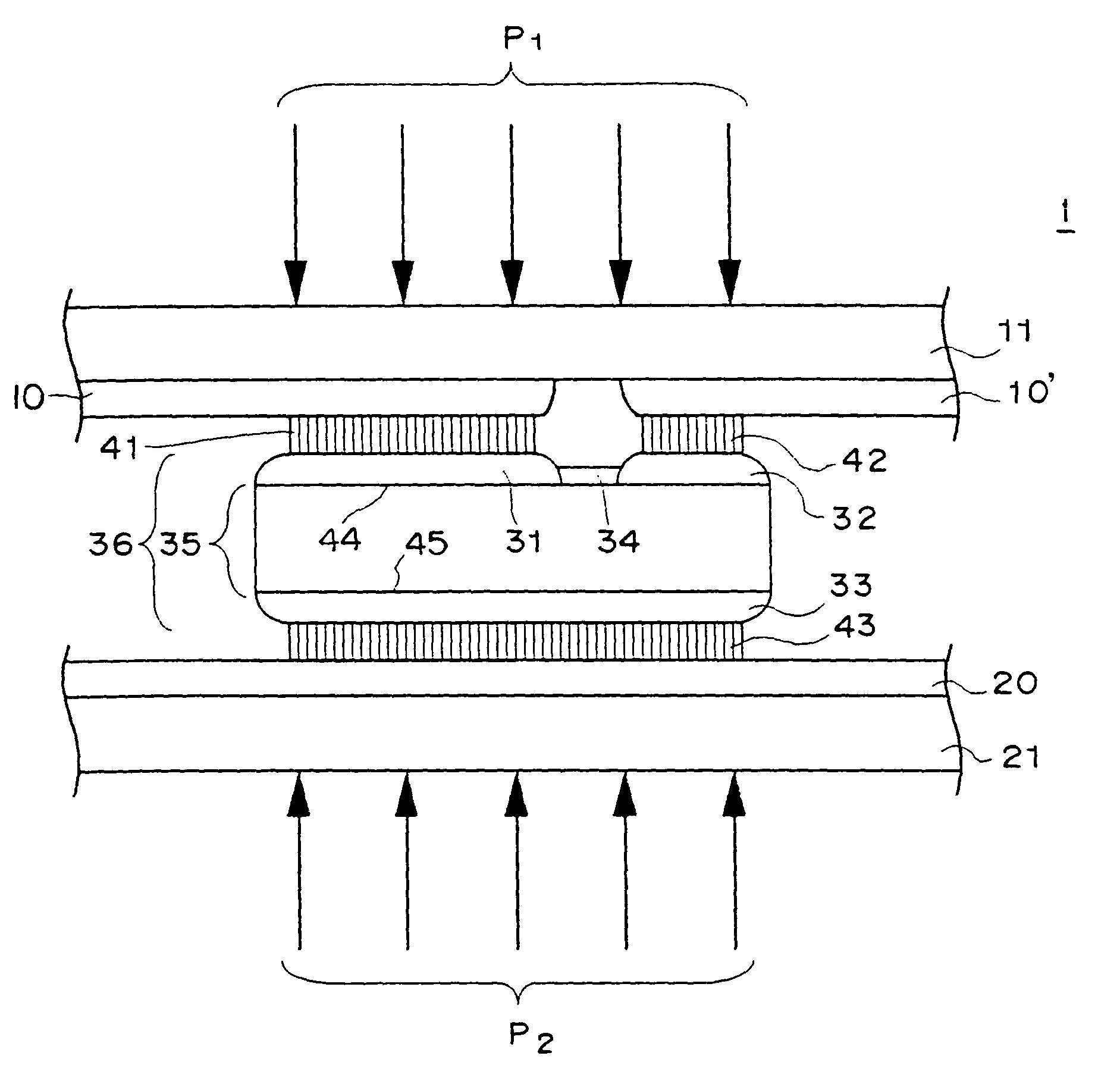
[0165]For the pressure-welded semiconductor device of Example 1, the semiconductor element 36′ shown in FIG. 4 manufactured by the above-described procedure was used to manufacture a pressure-welded semiconductor device where the pressure-welded portions between the semiconductor element and the casing had the configuration shown in FIG. 1.

[0166]The formation of the buffer conductive layers and the manufacture of the pressure-welded semiconductor device were conducted by the procedures described below.

Formation of the Buffer Conductive Layers

[0167]The semiconductor element 36′ was immersed for 10 seconds in an aqueous solution of sulfuric acid (10% by weight) in order to remove oxides from the surface of the emitter electrode 31 and the surfaces of the gate electrode 32 and the collector electrode 33. After the immersed semiconductor element 36′ was sufficiently rinsed and dried, the semiconductor element 36′ was placed in a reactor of an in-house manufactured CVD machine and air wa...

example 2

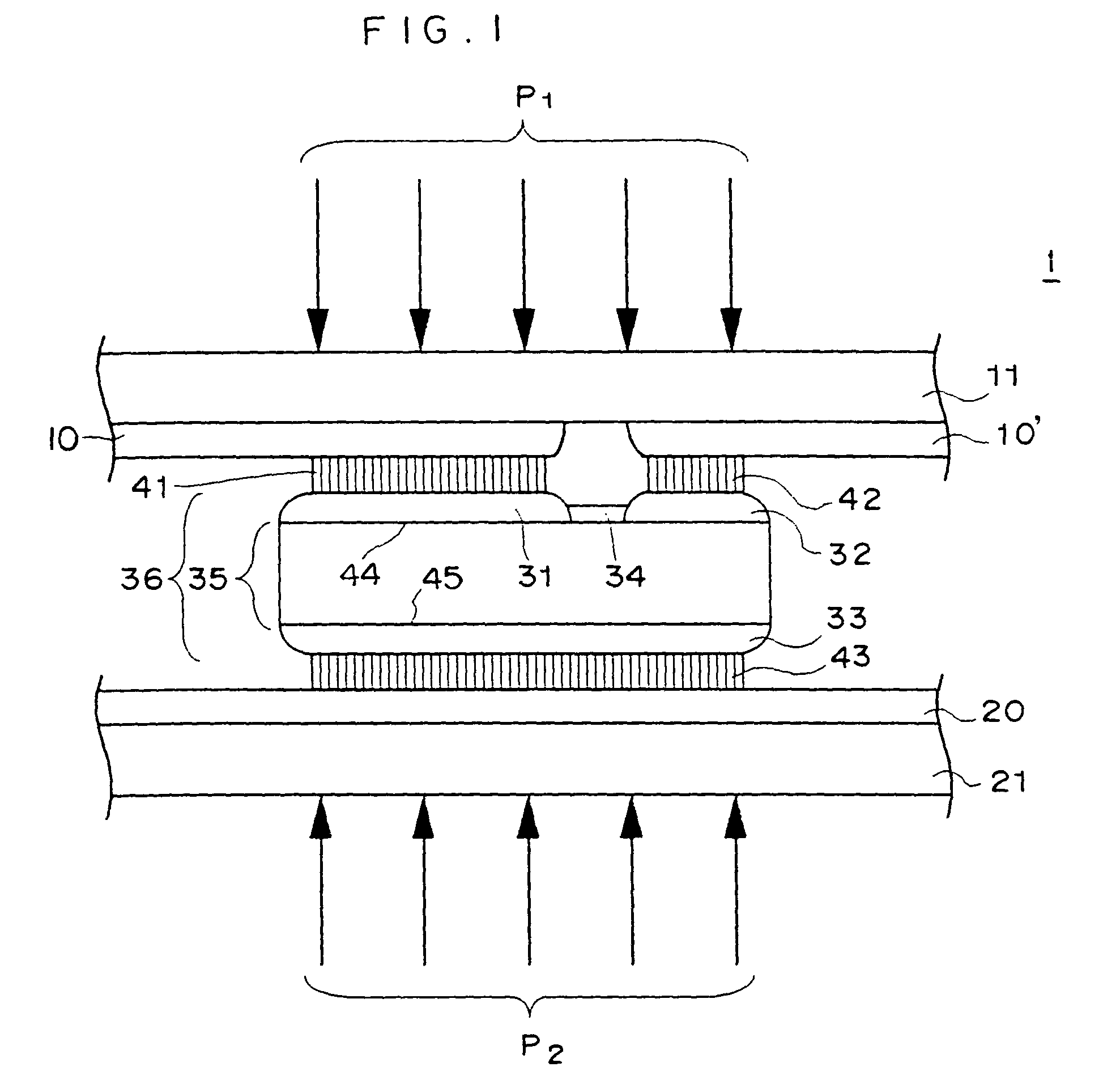
[0172]For the pressure-welded semiconductor device of Example 2, the semiconductor element 36′ shown in FIG. 4 manufactured by the above-described procedure was used to manufacture a pressure-welded semiconductor device where the pressure-welded portions between the semiconductor element and the casing had the configuration shown in FIG. 2.

[0173]The formation of the buffer conductive layers and the manufacture of the pressure-welded semiconductor device were conducted by the procedures described below.

Formation of the Buffer Conductive Layers

[0174]Using the semiconductor element 36′ where the surface of the gate electrode 32 was protected in advance with a resist, the semiconductor element 36′ was immersed for 10 seconds in an aqueous solution of sulfuric acid (10% by weight) in order to remove oxides from the surface of the emitter electrode 31 and the surfaces of the gate electrode 32 and the collector electrode 33. After the immersed semiconductor element 36′ was sufficiently rin...

example 3

[0182]For the pressure-welded semiconductor device of Example 3, the semiconductor element 36′ shown in FIG. 4 manufactured by the above-described procedure was used to manufacture a pressure-welded semiconductor device where the pressure-welded portions between the semiconductor element and the casing had the configuration shown in FIG. 1.

Formation of the Buffer Conductive Layers

[0183]The buffer conductive layers were manufactured in the same manner as the above Example 1.

Filling of the Carbon Nanotube Gaps with Metal

[0184]A wafer in which a film of carbon nanotubes was formed was immersed in diluted sulfuric acid, the nickel oxide films on the emitter electrode 31, the gate electrode 32 and the collector electrode 33, which were nickel electrodes, were removed and the metal nickel was exposed. Next, the wafer was immersed in a plating solution including nickel sulfate, lactic acid and sodium hypophosphate, and electroless nickel plating was conducted. Ni grew on the emitter electr...


PUM


Abstract

In a pressure-welded semiconductor device where at least one semiconductor element is disposed inside a casing, a buffer conductive layer including conductive carbons is disposed at pressure-welded portions between first casing-side electrodes and element-side electrodes disposed on a first main surface and at pressure-welded portions between second casing-side electrodes and element-side electrodes disposed on a second main surface.

Description

CROSS-REFERENCE TO RELATED APPLICATION[0001]This application claims priority under 35USC 119 from Japanese Patent Application No. 2002-266940, the disclosure of which is incorporated by reference herein.BACKGROUND OF THE INVENTION[0002]1. Field of the Invention[0003]The present invention relates to a pressure-welded semiconductor device using a semiconductor element.[0004]2. Description of the Related Art[0005]A pressure-welded semiconductor device has a structure where at least one electrode disposed on each of two main surfaces of a semiconductor element (hereinafter abbreviated as “element-side electrodes”), such as an insulating gate bipolar transistor (hereinafter abbreviated as an “IGBT”) or a MOS field-effect transistor (hereinafter abbreviated as a “MOSFET”), is pressurized by casing-side electrodes (hereinafter abbreviated as “casing-side electrodes”) that contact the element-side electrodes. The reliability of this pressure-welded semiconductor device is high because solde...

Claims


Application Information

Patent Timeline
Patent Type & Authority Patents(United States)
IPC IPC(8): H01L23/48H01L29/40H01L23/52B82B1/00H01L21/52H01L21/60H01L21/603H01L23/373H01L23/473H01L23/498H01L29/739H01L29/78H02H3/00
CPCH01L23/373H01L23/473H01L23/49833H01L23/49877H01L24/33H01L24/83H01L29/7395H01L2924/1305H01L2924/1306H01L2924/0132H01L2924/014H01L2924/01072H01L2924/01068H01L24/72H01L2224/291H01L2224/32014H01L2224/8319H01L2224/83801H01L2924/01004H01L2924/01005H01L2924/01011H01L2924/01013H01L2924/01015H01L2924/01018H01L2924/0102H01L2924/01027H01L2924/0103H01L2924/01039H01L2924/0104H01L2924/01042H01L2924/01046H01L2924/01057H01L2924/01058H01L2924/01059H01L2924/0106H01L2924/01064H01L2924/01074H01L2924/01078H01L2924/13055H01L2924/13091H01L2924/19042H01L2924/3025H01L2924/01006H01L2924/01019H01L2924/01023H01L2924/01033H01L2924/01045H01L2924/01065H01L2924/01066H01L2924/01067H01L2924/01029H01L2924/00H01L2924/12042
Inventor MIYACHI, YUKIOOKAMOTO, ATSUTO
Owner TOYOTA CENT RES & DEV LAB INC
Why Eureka
Try Eureka