Signal dividing circuit and semiconductor device

a signal dividing circuit and semiconductor technology, applied in the field of semiconductor devices, can solve the problems of signal reducing, signal being considerably blunted, signal not immediately dispensing, etc., and achieve the effect of limiting low production steps and costs and maintaining the function of signal processing thereo

Inactive Publication Date: 2006-01-31
SEMICON ENERGY LAB CO LTD
View PDF22 Cites 30 Cited by
  • Summary
  • Abstract
  • Description
  • Claims
  • Application Information

AI Technical Summary

Benefits of technology

[0026]It is a problem of the present invention disclosed in the specification to provide a constitution in a semiconductor device with a digita...

Problems solved by technology

However, under such a high frequency condition, function of a transistor in the drive circuit is insufficient, the operation of the circuit is not feasible or devoid of reliability.
However, even when the function of the transistor in the drive circuit is promoted, the signal dividing circuit is not immediately dispensed with.
Firstly, there is a problem caused by resistance or capacitance.
Then, when the frequency of a signal transmitted from outside is high, there may cause a hazard in normally operating the drive circuit such that the signal becomes considerably blunted in the drive circuit, when a voltage value of the power source line is instantaneously changed by influence of certain operation in the drive circuit, a time period permitted for the recovery becomes deficient and so on.
Therefore, the shift register may not be operated normally when the bluntness of the clock signal exceeds a limit at a midway and the clock signal cannot be read at a predetermined timing.
Secondary, the...

Method used


Image

  • Signal dividing circuit and semiconductor device
  • Signal dividing circuit and semiconductor device
  • Signal dividing circuit and semiconductor device

Examples


embodiment 1

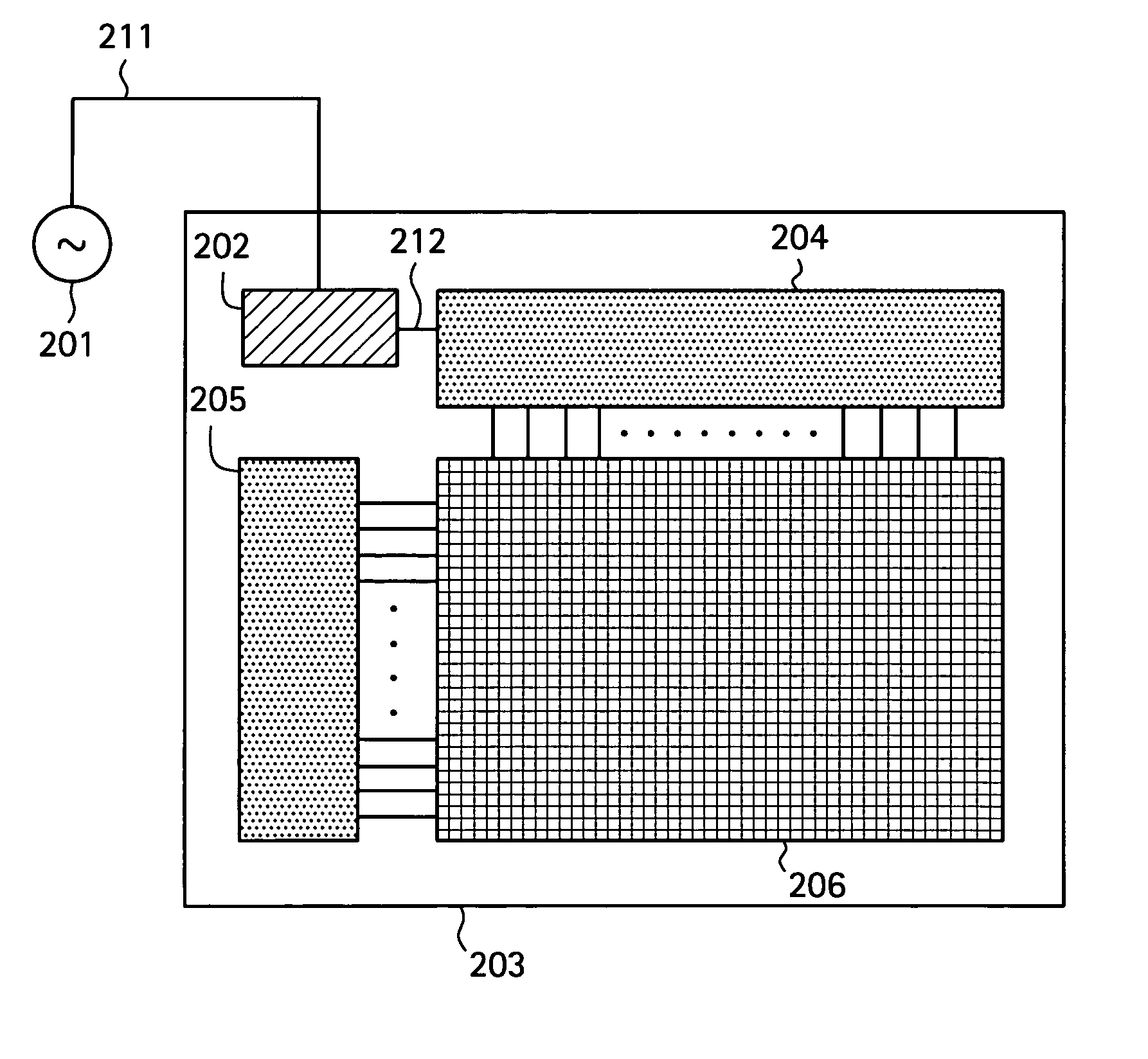
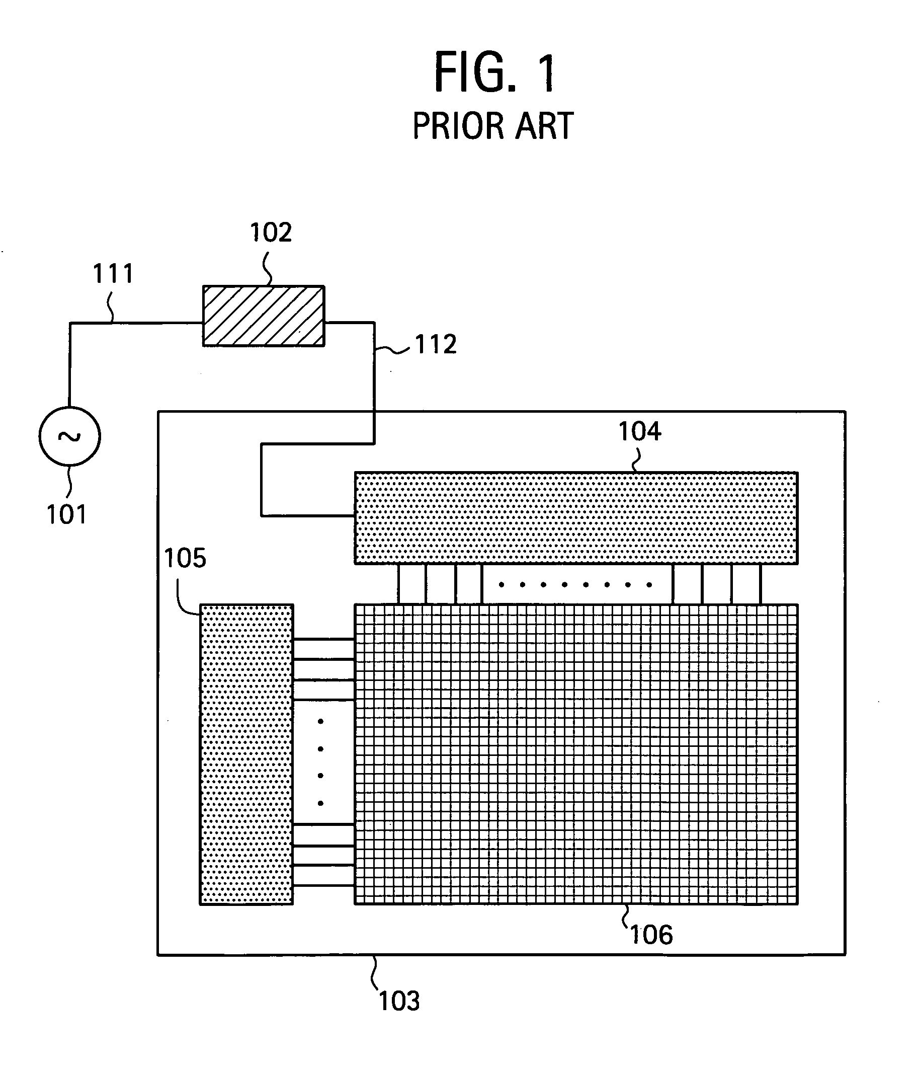
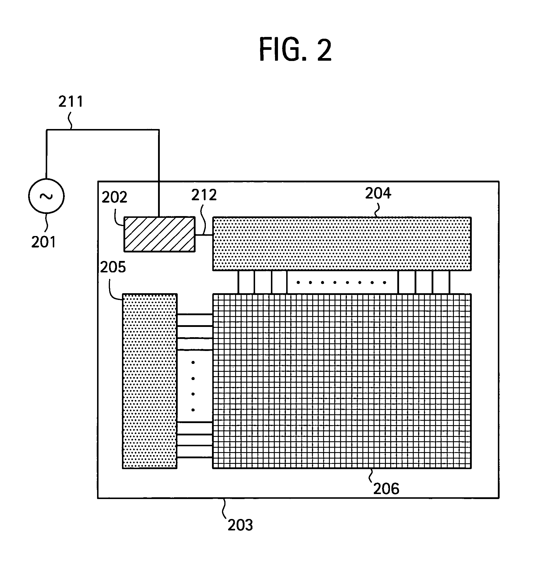
[0063]FIG. 2 shows a constitution block diagram of an embodiment according to the present invention. This is an example which is applied to a liquid crystal display device with a digital signal as an input signal. A signal dividing circuit 202 is constituted by TFTs and is formed on a same substrate integrally with circuits of a pixel matrix unit 206 and a signal line drive circuit 204 and a scanning line drive circuit 205. In the FIG. 2, numeral 201 shows a digital signal source, numeral 203 shows a substrate having an insulating surface; for example, a glass, a quartz and so on. Numeral 211 shows an input digital signal line, numeral 212 shows a modified digital signal line.

[0064]FIG. 3A shows a constitution diagram of the signal dividing circuit 202. It is assumed in the embodiment that the number n of input digital signal lines is set to 1, the number m of signal divisions is set to 4 and an input digital signal is of 80 MHz (in correspondence with picture image display under XG...

embodiment 2

[0181]In this embodiment, an explanation will be given of a case in which the input digital signal number n is set to 1 and the signal division number m is set to 8 in the signal dividing circuit according to the present invention shown by FIGS. 3A and 3B. Further, the frequency of the input digital signal is set to 80 MHz. Further, fabrication method follows the method of Embodiment 1.

[0182]FIG. 16 shows a result of measuring operation of the signal dividing circuit of the embodiment by an oscilloscope. An explanation will be given of respective signal waveforms. In this case, an explanation will be given of respective signal waveforms by using notations (1, 2, 3, R1, R2, R3) on the left of the respective signal waveforms.

[0183]The signal waveform 1 monitors a reset signal. The signal waveform 2 monitors a clock signal. The signal waveform R1 monitors the input digital signal. In this embodiment, as mentioned above, the frequency of the input digital signal is set to 80 MHz. The si...


PUM


Abstract

To provide a constitution capable of reducing production cost in a semiconductor device for display of a type integrally formed with a drive circuit with a digital signal as an input signal and a pixel matrix unit, a signal dividing circuit is formed on a substrate where drive circuits and a pixel matrix unit are to be formed simultaneously with the drive circuits and the pixel matrix unit in view of fabrication steps by which fabrication steps of the signal dividing circuit per se and steps required for connecting the signal dividing circuit to wirings on the substrate can be dispensed with without adding further steps.

Description

BACKGROUND OF THE INVENTION[0001]1. Field of the Invention[0002]The present invention disclosed in the specification relates to a semiconductor device with a digital signal as an input signal. For example, the present invention can be utilized in a liquid crystal display device of an active matrix type, an EL (electroluminescence) display device and so on. More accurately, the present invention can be utilized in a drive substrate of a liquid crystal display device of an active matrix type, an EL display device and the like.[0003]2. Description of Related Art[0004]There is provided a liquid crystal display device of an active matrix type as an example of a semiconductor device with a digital signal as an input signal.[0005]Conventionally, a liquid crystal display device of an active matrix type with a digital signal as an input signal is provided with a constitution as shown by FIG. 1.[0006]A signal dividing circuit 102 receives an input of a digital signal for constituting an input...

Claims


Application Information

Patent Timeline
IPC IPC(8): G09G3/36G02F1/136G02F1/1368G09F9/00H01L21/336H01L21/77H01L21/84H01L27/12H01L29/786
CPCH01L27/1214G09G3/3275G09G3/3611G09G2300/0408G09G2310/0275G09G2320/0233G09G2310/027H01L27/1277
Inventor KOYAMA, JUNOSAME, MITSUAKIOGATA, YASUSHI
Owner SEMICON ENERGY LAB CO LTD
Why Eureka
Try Eureka