Semiconductor manufacturing apparatus control system

a control system and semiconductor technology, applied in the direction of semiconductor/solid-state device testing/measurement, photomechanical apparatus, instruments, etc., can solve the problems of reducing the price of products that can be mass-produced, such as memories, and the stop of wafer transportation, so as to achieve the effect of eliminating the stop time of wafer transportation and increasing the availability and throughput of the stepper

Inactive Publication Date: 2006-02-07
ASAHI KASEI ELECTRONICS CO LTD
View PDF7 Cites 12 Cited by
  • Summary
  • Abstract
  • Description
  • Claims
  • Application Information

AI Technical Summary

Benefits of technology

[0029]With such an arrangement, when it is determined that said second group of wafers can be transported to the exposure stage following said first group of wafers, said stepper starts transportation of said second wafers im

Problems solved by technology

However, in recent years, products that can be mass-produced, such as memories, tend to decrease in price, and thus, attentions of many semiconductor manufacturers has been shifted to manufacture of high-value-added custom products.
However, since transportation of wafers is stopped every time exposure of all the wafers housed in one cassette is completed, for example, even if the wafers processed according to the same process recipe cannot be

Method used


Image

  • Semiconductor manufacturing apparatus control system
  • Semiconductor manufacturing apparatus control system
  • Semiconductor manufacturing apparatus control system

Examples


Embodiment Construction

[0037]An embodiment of a stepper control system according to the invention will be described below with reference to the drawings.

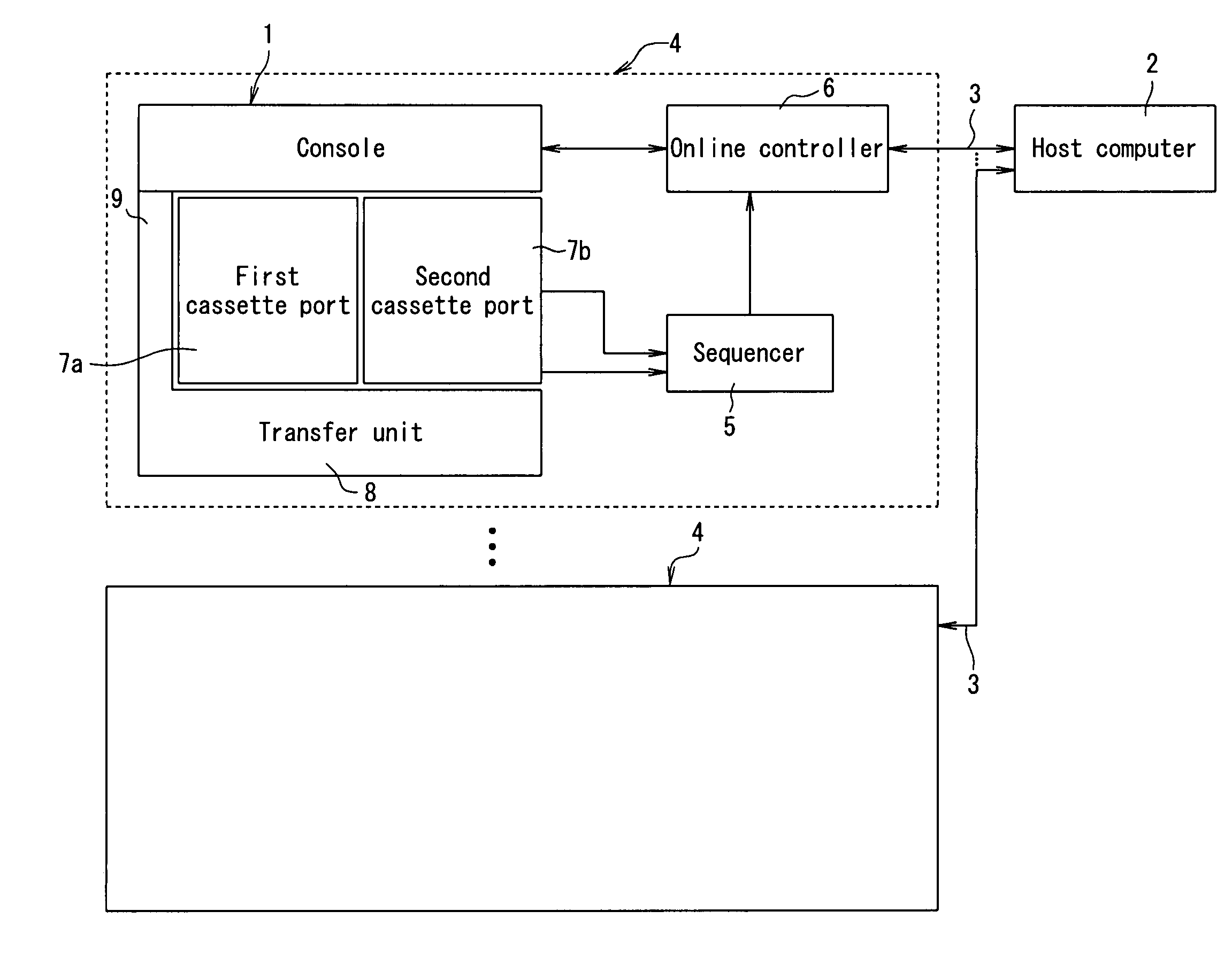
[0038]FIG. 1 is a schematic diagram showing an arrangement of the stepper control system according to the invention. As shown in FIG. 1, the stepper control system comprises one host computer 2 storing correspondences between lot numbers and process recipes and a plurality of exposure stations 4 connected to the host computer 2 via a communication line 3.

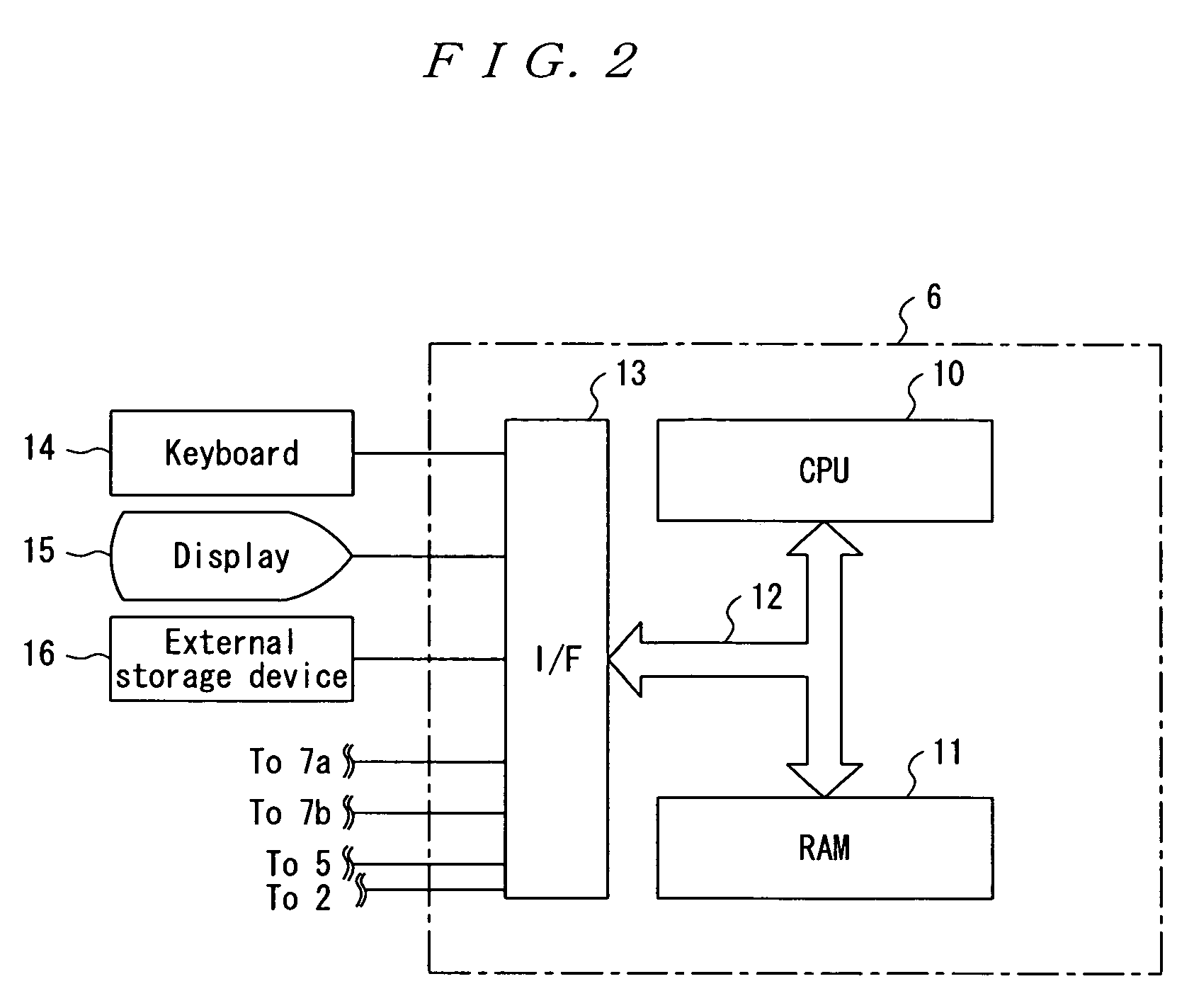
[0039]The exposure station 4 comprises a plurality of devices for obtaining a process recipe from the host computer 2 and sequentially performs exposure. It comprises a stepper 1 for performing exposure of a semiconductor wafer, a sequencer 5 connected to the stepper 1 for detecting the progress of the exposure from the stepper 1, and an online controller 6 connected to the host computer 2, the stepper 1 and the sequencer 5 for obtaining the process recipe from the host computer 2 and the progress informa...


PUM


Abstract

To reduce a stop time of transportation of wafers which occurs when one stepper handles many kinds of products, before exposure of semiconductor wafers of a first cassette port 7a is completed, a process recipe for semiconductor wafers of a second cassette port 7b is obtained from a host computer 2, the progress of the exposure of the semiconductor wafers of the first cassette port 7a is detected via a sequencer 5, it is determined, based on the obtained process recipe, whether or not the semiconductor wafers of the second cassette port 7b can be transported to an exposure stage following the last semiconductor wafer of the first cassette port 7a, and a stepper 1 is caused to perform exposure in accordance with the determination result and the progress detection result.

Description

TECHNICAL FIELD[0001]The present invention relates to a control system for a semiconductor manufacturing apparatus that controls the semiconductor manufacturing apparatus, such as a stepper, that transfers a pattern on a reticle to a wafer based on information obtained from a host computer.BACKGROUND ART[0002]A conventionally known manufacturing line that performs a photolithographic process on a semiconductor device, liquid crystal display element or the like comprises, as shown in FIG. 6, a plurality of steppers 1 and one host computer 2 for controlling the plurality of steppers 1, the steppers and the host computer being connected to each other via a communication line 3.[0003]In such a manufacturing line, each stepper 1 is adapted to perform an exposure process under the control of the host computer 2. First, an operator manipulates an online terminal for the host computer to obtain a process recipe from the host computer 2. Then, after a reticle is set in a reticle library capa...

Claims


Application Information

Patent Timeline
IPC IPC(8): G06F19/00G03F7/20H01L21/00H01L21/66
CPCG03F7/70525G03F7/7075H01L21/67276H01L22/20Y10T29/41H01L2924/0002H01L2924/00H01L21/027
Inventor IMAI, KEIJI
Owner ASAHI KASEI ELECTRONICS CO LTD
Why Eureka
Try Eureka