Ion implanter having two-stage deceleration beamline

Inactive Publication Date: 2006-02-14
VARIAN SEMICON EQUIP ASSOC INC
View PDF24 Cites 61 Cited by
  • Summary
  • Abstract
  • Description
  • Claims
  • Application Information

AI Technical Summary

Benefits of technology

[0018]The first and second deceleration stages may each include a deceleration electrode for decelerating ions in the ion beam and a suppression electrode for suppressing flow of electrons in the ion beam from one ene

Problems solved by technology

However, ion implanters are typically designed for efficient operation at relatively high implant energies, for example in the range of 20 keV to 400 keV, and may not function efficiently at the energies required for shallow junction implantation.
As a result, extremely long implant times are required to achieve a specified dose, and throughput is adversely affected.
Such reduction in throughput increases fabrication cost and is unacceptable to semiconductor device manufacturers.
However, a small ion current is delivered to the wafer because the ion source operates inefficiently at low extraction voltages.
This approach also suffers from ion beam expansion and energy contamination in the beam delivered to the wafer.
Delivery of low (less than 10 keV) and ultra-low (less than 1 keV) energy, mass resolved, m

Method used


Image

  • Ion implanter having two-stage deceleration beamline
  • Ion implanter having two-stage deceleration beamline
  • Ion implanter having two-stage deceleration beamline

Examples


Embodiment Construction

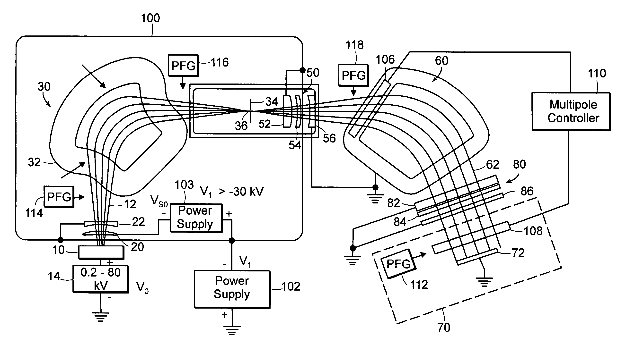
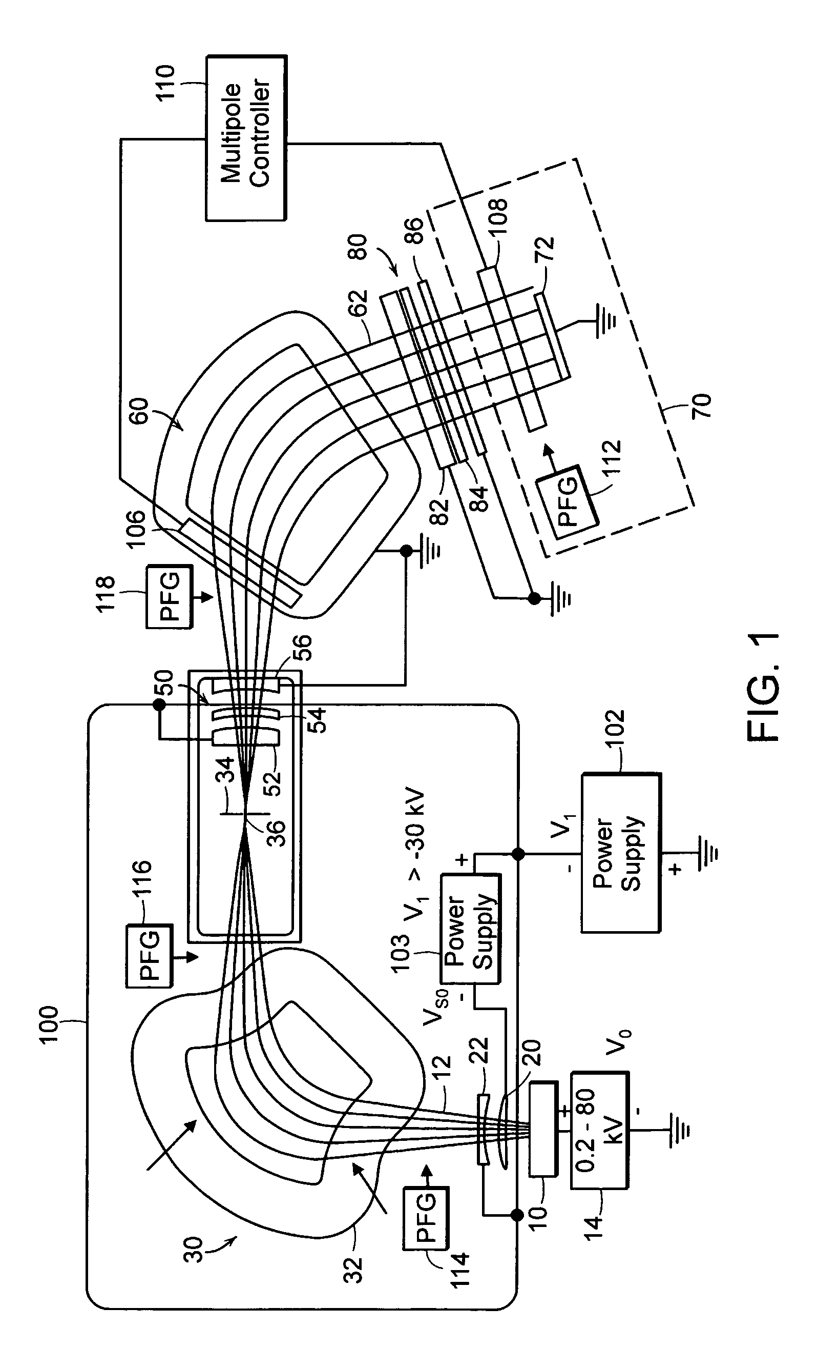
[0032]A block diagram of an ion implanter in accordance with an embodiment of the invention is shown in FIG. 1. An ion source 10 generates ions and supplies an ion beam 12. As known in the art, ion source 10 may include an ion chamber and a gas box containing a gas to be ionized. The gas is supplied to the ion chamber where it is ionized. The ions thus formed are extracted from the ion chamber to form ion beam 12. Ion beam 12 has an elongated cross section and is ribbon-shaped, with a long dimension of the beam cross section preferably having a horizontal orientation. A first power supply 14 is connected to an extraction electrode of ion source 10 and provides a positive first voltage V0. First voltage V0 may be adjustable, for example, from about 0.2 to 80 kV. Thus, ions from ion source 10 are accelerated to energies of about 0.2 to 80 keV by the first voltage V0. The construction and operation of ion sources are well known to those skilled in the art.

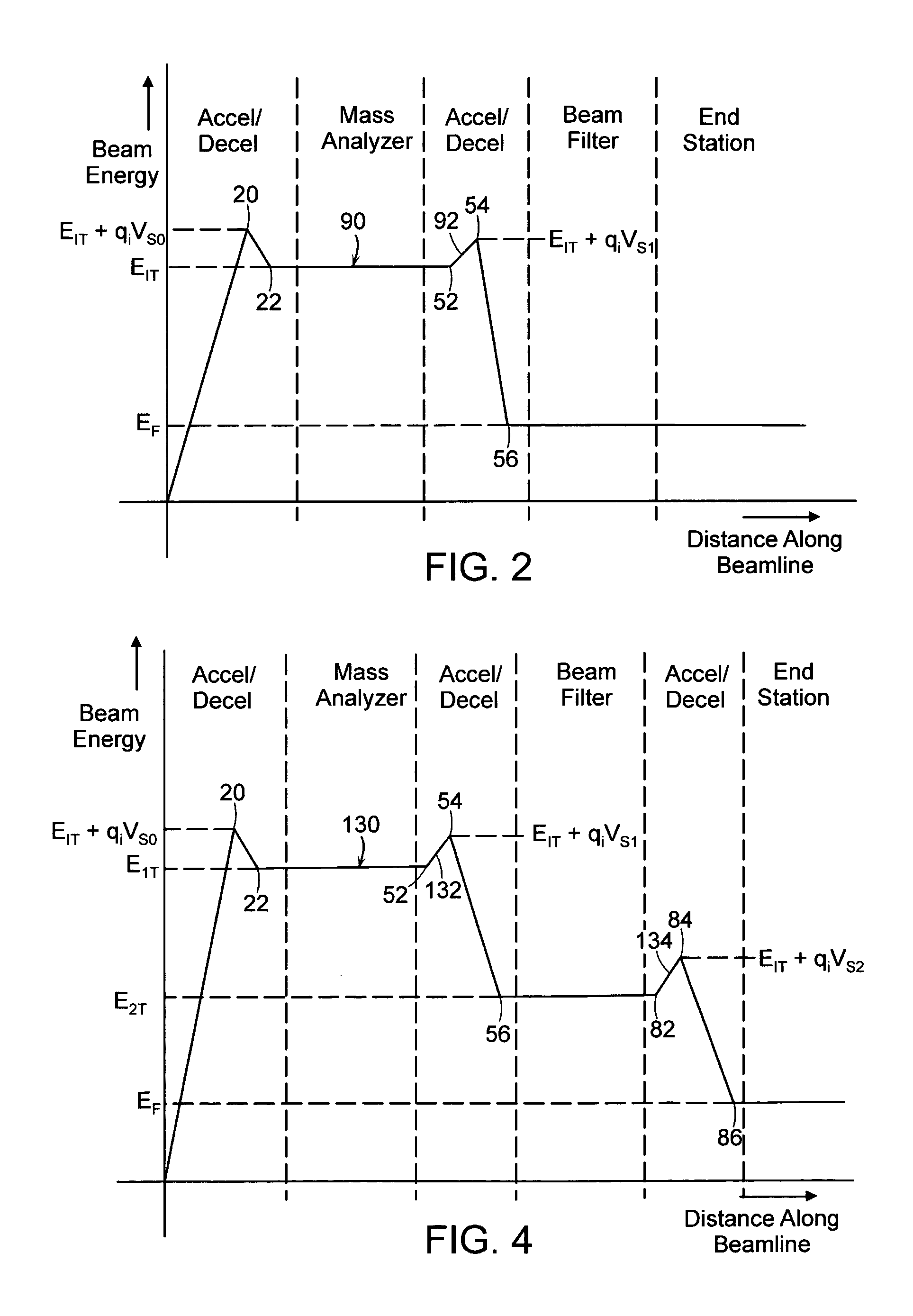
[0033]Ion beam 12 passes throu...


PUM


Abstract

An ion implanter includes an ion source for generating an ion beam, an analyzer for separating unwanted components from the ion beam, a first beam transport device for transporting the ion beam through the analyzer at a first transport energy, a first deceleration stage positioned downstream of the analyzer for decelerating the ion beam from the first transport energy to a second transport energy, a beam filter positioned downstream of the first deceleration stage for separating neutral particles from the ion beam, a second beam transport device for transporting the ion beam through the beam filter at the second transport energy, a second deceleration stage positioned downstream of the beam filter for decelerating the ion beam from the second transport energy to a final energy, and a target site for supporting a target for ion implantation. The ion beam is delivered to the target site at the final energy. In a double deceleration mode, the second transport energy is greater than the final energy for highest current at low energy. In an enhanced drift mode, the second transport energy is equal to the final energy for highest beam purity at low energy.

Description

CROSS REFERENCE TO RELATED APPLICATION[0001]This application claims the benefit of provisional application Ser. No. 60 / 140,466 filed Jun. 23, 1999, which is hereby incorporated by reference.FIELD OF THE INVENTION[0002]This invention relates to systems and methods for ion implantation and, more particularly, to methods and apparatus for delivery of low energy, monoenergetic ion beams to an ion implantation target, such as a semiconductor wafer.BACKGROUND OF THE INVENTION[0003]Ion implantation has become a standard technique for introducing conductivity-altering impurities into semiconductor wafers. A desired impurity material is ionized in an ion source, the ions are accelerated to form an ion beam of prescribed energy and the ion beam is directed at the surface of the wafer. The energetic ions in the beam penetrate into the bulk of the semiconductor material and are embedded into the crystalline lattice of the semiconductor material to form a region of desired conductivity.[0004]Ion...

Claims


Application Information

Patent Timeline
IPC IPC(8): G21K5/10H01J37/08
CPCH01J37/3171H01J2237/0041H01J2237/31705H01J2237/047H01J2237/022
Inventor MCKENNA, CHARLES M.WHITE, NICHOLAS R.BROWN, DOUGLAS A.BELL, EDWARDRADOVANOV, SVETLANA
Owner VARIAN SEMICON EQUIP ASSOC INC
Why Eureka
Try Eureka