Semiconductor optical device

a semiconductor and optical device technology, applied in the direction of semiconductor lasers, optical resonator shape and construction, active medium materials, etc., can solve the problems of waveguide instability, waveguide instability, linearity between current and optical output adversely affected, and the transverse mode of laser oscillation, etc., to reduce the variation of refractive index across the beam waveguide

Inactive Publication Date: 2006-02-14
MITSUBISHI ELECTRIC CORP
View PDF3 Cites 11 Cited by
  • Summary
  • Abstract
  • Description
  • Claims
  • Application Information

AI Technical Summary

Benefits of technology

[0013]One of the aspects of the present invention is to provide a semiconductor optical device including a beam waveguide extending in a longitudinal direction between a pair of end surfaces. The beam waveguide includes an active layer of a quantum well structure having at least one well and barrier layers, and a pair of cladding layers sandwiching

Problems solved by technology

Because of this result, when the variation of the refractive index across the oscillator (active layer 3) is too broad, the transverse mode of the laser oscillation, influenced by the difference of refractive index between the core portion and the cladding portion of the beam waveguide, becomes unstable.

Method used


Image

  • Semiconductor optical device
  • Semiconductor optical device
  • Semiconductor optical device

Examples


embodiment 1

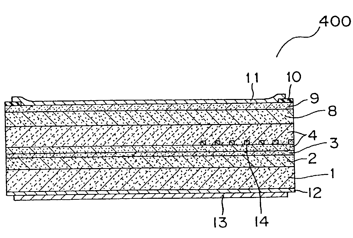
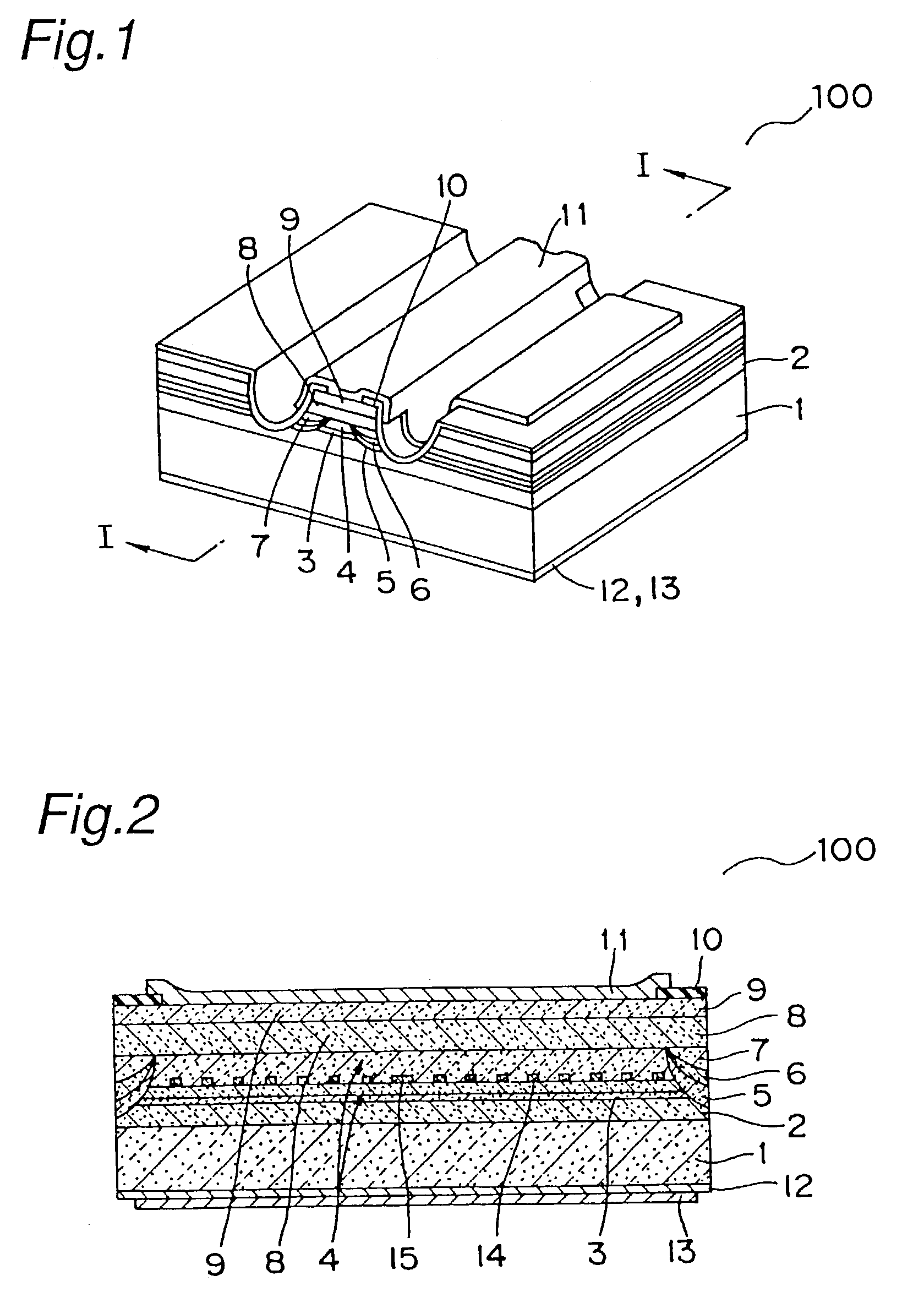
[0039]FIG. 1 is a perspective view of a λ / 4-shifted distributed-feedback semiconductor laser device according to the first embodiment of the present invention. FIG. 2 is a cross sectional view taken along a line II—II of FIG. 1. In FIGS. 1 and 2, the same reference numerals denote the same elements.

[0040]With reference to FIGS. 1 and 2, in particular, the distributed-feedback semiconductor laser device 100 includes a substrate 1 of p-InP, on which a buffer layer (or first cladding layer) 2 of p-InP is formed. Formed on the buffer layer 2 is an active layer 3 formed as a multiple quantum well (MQW) layer of InGaAsP. The active layer 3 may be formed as a single quantum well (SWQ) layer. Also, provided on the active layer 3 are cladding layers 4, 8 of n-InP. The active layer 3 is sandwiched between the buffer layer 2 and the cladding layer 4.

[0041]Further, grown adjacent to both end surfaces are blocking layers 5, 7 of p-InP and a blocking layer 6 of n-InP sandwiched therebetween.

[0042...

example 1

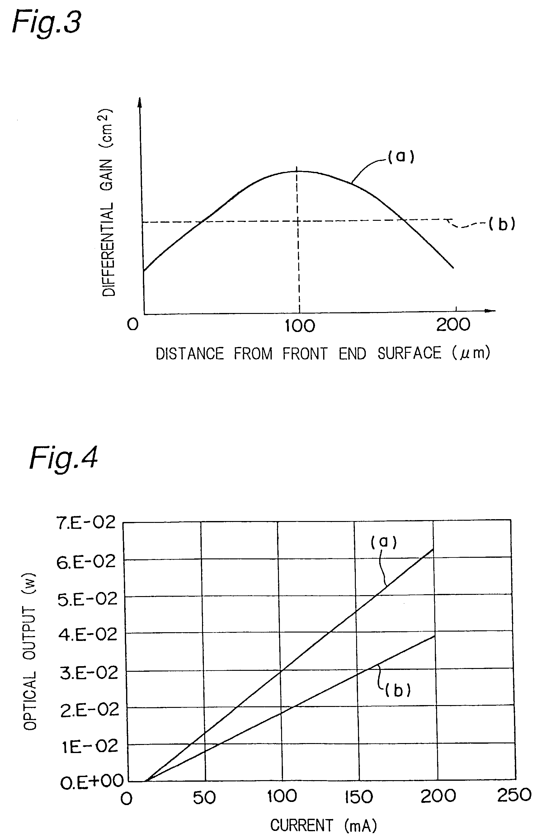
[0058]In the first example of the present embodiment, the distributed-feedback semiconductor laser device 100 shown FIGS. 1 and 2 is designed so that a plurality: of quantum well layers of the active layer 3 has thickness modified to be thinner in the regions adjacent to the middle point than both end surfaces. Thus, the differential gain is increased in the region adjacent to the middle point between both end surfaces so that the variation of the refractive index across the beam waveguide is reduced.

[0059]FIG. 8 is a graph illustrating the thickness of the well layer for the distance from the front-end surface of the distributed-feedback semiconductor laser device 100 according to the first example. The distributed-feedback semiconductor laser device 100 according to the first example has the well layer modified so that it gradually and continuously becomes thinner towards the middle point as shown by the solid line (a). Meanwhile, the conventional distributed-feedback semiconducto...

example 2

[0074]In the distributed-feedback semiconductor laser device 100 of the second example, the oscillation wavelength is determined by the space of the adjacent diffraction gratings, while the maximum gain wavelength is defined by a composition material of the active layer 3. Therefore, a detuning wavelength can be defined herein as a difference between the oscillation wavelength and the maximum gain wavelength.

[0075]In the second example, the distributed-feedback semiconductor laser device 100 is designed so that the detuning wavelength thereof is increased in the first region adjacent to the middle point between both end surfaces where the photon density within the oscillator (active layer 3) is increased. To this end, the differential gain in the first region adjacent to the middle point between both end surfaces can be increased.

[0076]FIG. 12 is a graph illustrating relationship between the state density and the energy level. Electrons are allowed to exist in the hatched region in ...


PUM


Abstract

A kink-free semiconductor optical device stabilizing laser oscillation and producing a high optical performance. The semiconductor optical device includes a beam waveguide extending in a longitudinal direction between a pair of end surfaces. The beam waveguide includes an active layer having a quantum well structure with at least one well layer and two barrier layers, and a pair of cladding layers sandwiching the active layer. The active layer has first and second regions in the longitudinal direction, the photon density in the first region being larger than in the second region. The first region has a differential gain greater than the second region so that variation of refractive index across the beam waveguide is reduced.

Description

BACKGROUND OF THE INVENTION[0001]1) Technical field of the Invention[0002]The present invention relates to a semiconductor optical device, and in particular, relates to a semiconductor optical device used for an optical communication system and an optical disc device.[0003]2) Description of Related Arts[0004]Referring to FIGS. 21 and 22, a semiconductor optical device as denoted by numerical reference 500 according to the prior art will be described hereinafter. FIG. 21 is a perspective view of a λ / 4-shifted distributed-feedback semiconductor laser device 500 as an example of the semiconductor optical device, and FIG. 22 is a cross sectional view taken along the line of XXII—XXII of FIG. 21.[0005]The distributed-feedback semiconductor laser device 500 includes, in general, a buffer layer 2, and an active layer 3 subsequently formed on a substrate 1. The active layer 3 is a multiple quantum well (MQW) layer. Also provided on the active layer 3 are cladding layers 4 and 8. The active ...

Claims


Application Information

Patent Timeline
IPC IPC(8): H01S3/13H01S3/08H01S3/14H01S5/00H01S5/34H01S5/12H01S5/16H01S5/227
CPCH01S5/10H01S5/101H01S5/2272H01S5/12H01S5/168H01S5/106
Inventor TAKAGI, KAZUHISA
Owner MITSUBISHI ELECTRIC CORP
Why Eureka
Try Eureka