Method of forming a non-volatile electron storage memory and the resulting device

a non-volatile, electron storage technology, applied in the direction of semiconductor devices, instruments, electrical apparatus, etc., can solve the problems of preventing preventing low voltage operation, affecting the operation of memory devices, etc., to eliminate the need for costly mask steps

Inactive Publication Date: 2006-02-28
MICRON TECH INC
View PDF10 Cites 137 Cited by
  • Summary
  • Abstract
  • Description
  • Claims
  • Application Information

AI Technical Summary

Benefits of technology

[0008]The invention provides a method of forming a semiconductor device and the resulting device which mitigates the foregoing problems. The device comprises a gate structure having a first gate insulating layer formed over a semiconductor substrate and a electron trapping layer containing a noble metal formed over the first gate insulating layer. Preferably, the noble metal is formed of platinum, rhodium, or ruthenium which enables self-forming nano-crystals. The self-forming nano-crystals eliminate the need for costly mask steps to form the nano-crystals. Further, the gate structure includes a second gate insulating layer formed over the electron trapping layer. In a preferred embodiment of the invention, the first gate oxide is preferably SiO2 (silicon dioxide), but a high dielectric constant advanced dielectric, such as Ta2O5 (tantalum oxide), BaSrTiO3 (barium strontium titanate), HfO2 (hafnium oxide), or ZrO2 (zirconium oxide) can also be used. The gate structure further includes a gate electrode formed on the second gate insulating layer. Source and drain regions are provided in surface portions of the semiconductor substrate with the gate structure between them.

Problems solved by technology

The SiO2 gate oxide has a dielectric constant of 3.9 which does not allow scaling and also does not permit low voltage operation.
Also, depending on what control gate oxide is used and subsequent processing steps used, the silicon nano-crystals could oxidize, which would impede or destroy memory device operation.
For example, if a high constant (high-K) dielectric, such as Ta205, is used as the control gate oxide to scale the gate threshold voltage for low voltage application, formation of the Ta205 control gate oxide could oxidize the silicon nano-crystals destroying the memory cell.

Method used


Image

  • Method of forming a non-volatile electron storage memory and the resulting device
  • Method of forming a non-volatile electron storage memory and the resulting device
  • Method of forming a non-volatile electron storage memory and the resulting device

Examples


Embodiment Construction

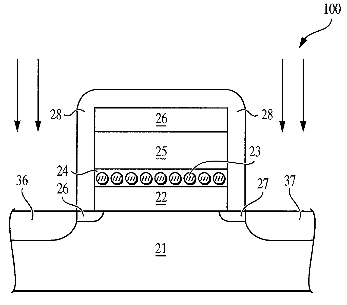
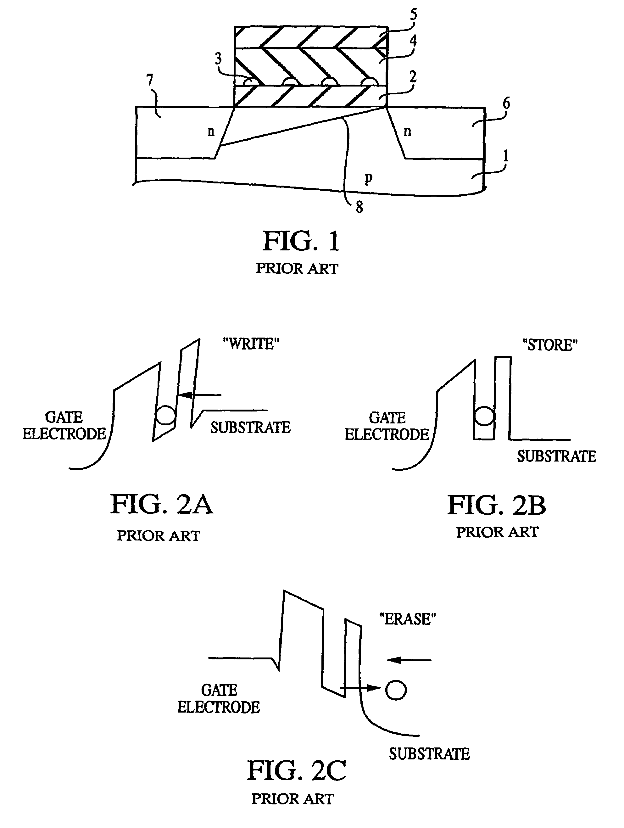
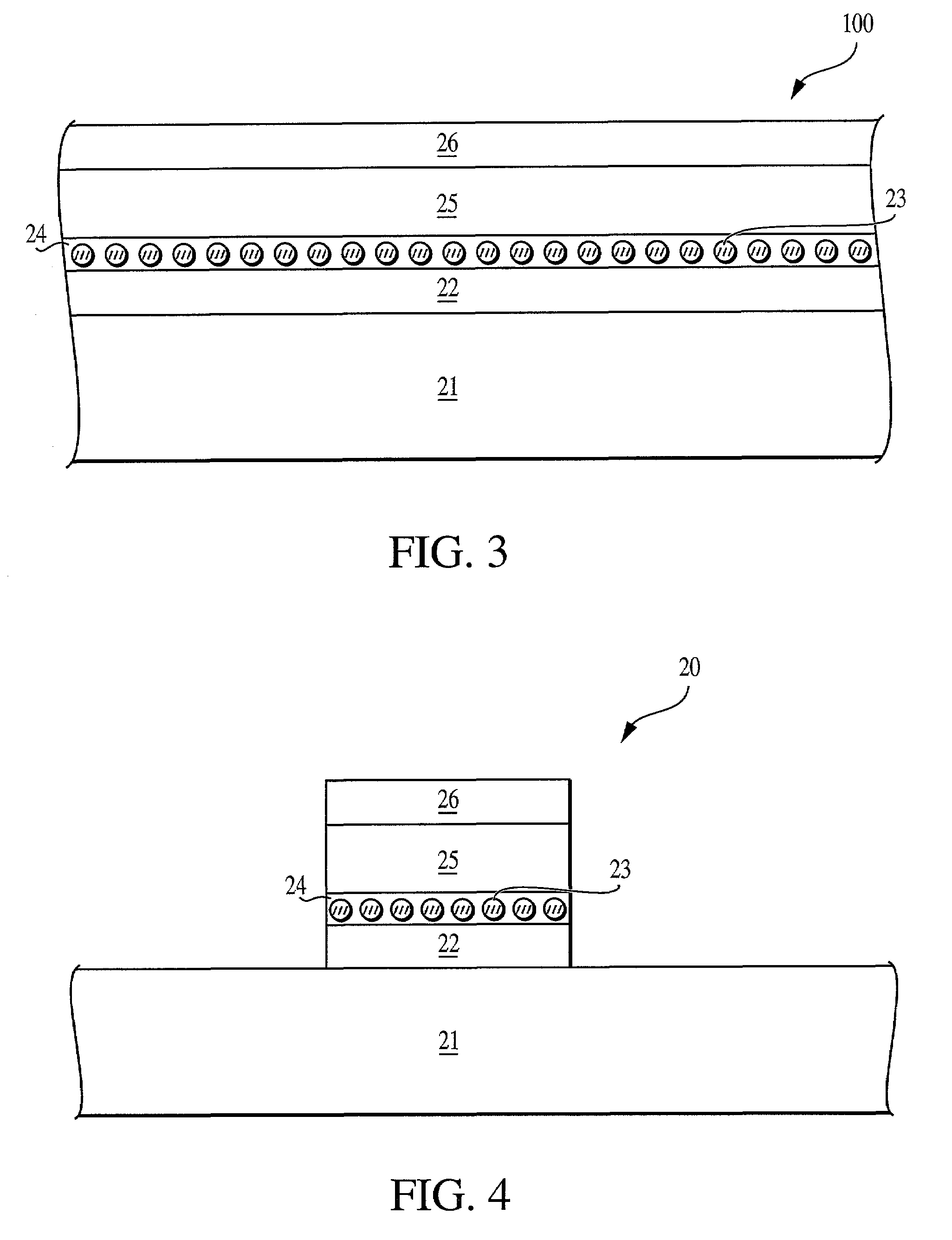
[0018]In the following detailed description, reference is made to various exemplary embodiments of the invention. These embodiments are described with sufficient detail to enable those skilled in the art to practice the invention, and it is to be understood that other embodiments may be employed, and that structural and electrical changes may be made without departing from the spirit or scope of the invention. As the skilled person will readily appreciate, these figures are merely of an illustrative nature and are provided only to facilitate the explanation of various process steps. Accordingly, the relation between various feature sizes may not necessarily reflect the real situation. In addition, in reality, boundaries between specific portions of the device and between various layers may not be as sharp and precise as illustrated in these figures.

[0019]The term “substrate” used in the following description may include any semiconductor-based structure that has an exposed semicondu...


PUM


Abstract

The invention provides a method of forming an electron memory storage device and the resulting device. The device comprises a gate structure which, in form, comprises a first gate insulating layer formed over a semiconductor substrate, a self-forming electron trapping layer of noble metal nano-crystals formed over the first gate insulating layer, a second gate insulating layer formed over the electron trapping layer, a gate electrode formed over the second gate insulating layer, and source and drain regions formed on opposite sides of the gate structure.

Description

FIELD OF INVENTION[0001]This invention relates to integrated circuit memory devices, and, more particularly, to a method and device for providing high-density, high-storage capacity, low-power, non-volatile memory devices.BACKGROUND OF THE INVENTION[0002]Non-volatile memory devices which store electrons in nano-crystals instead of floating gates, are presently of great interest, due to potential advantages in memory cell size and power dissipation, compared to memory technologies currently in use. The use of nano-crystals for electron storage will provide greater reliability and low-voltage operation. Research in this area is reported in the article “Volatile and Non-Volatile Memories in Silicon with Nano-Crystal Storage” by Tiwasi et al., IEEE, IEDM, 1995, pgs. 521–524, the disclosure of which is incorporated herein by reference.[0003]FIG. 1 is a sectional view illustrating a floating-gate n-channel MOS electron memory device. In the figure, reference numeral 1 denotes a silicon (S...

Claims


Application Information

Patent Timeline
Patent Type & Authority Patents(United States)
IPC IPC(8): H01L29/788G11C16/04H01L21/28H01L21/336H01L29/423H01L29/51
CPCB82Y10/00H01L21/28185H01L21/28194H01L29/42332H01L29/513H01L29/517H01L29/66825H01L29/7883H01L21/28273G11C16/0416G11C2216/06Y10S977/943H01L29/40114
Inventor BATRA, SHUBNEESHSANDHU, GURTEJ
Owner MICRON TECH INC
Why Eureka
Try Eureka