Unilateral thermal buckle beam actuator

a technology of actuators and thermal buckles, applied in the direction of mechanical equipment, generators/motors, machines/engines, etc., can solve the problems of large actuation displacement, large actuation displacement, and small actuation energy, and achieve long actuation displacement, small area, and high force

Inactive Publication Date: 2006-03-07
MICROSOFT TECH LICENSING LLC
View PDF76 Cites 17 Cited by
  • Summary
  • Abstract
  • Description
  • Claims
  • Application Information

AI Technical Summary

Benefits of technology

[0009]The resistivity of polysilicon allows the actuator b operate at voltages and currents compatible with standard integrated circuitry (e.g., CMOS). In addition, actuators according to the present invention are very small in area, have relatively high force, and can provide relatively long actuation displacements (e.g. 10–20 microns) at very small increments, making them suitable for deployment of MEMS devices as well as providing minute adjustments in MEMS systems. In one implementation, the present actuator array can produce a force of about 3700 μN per square mm and with 1.53 mW per μN of power. This electrically stimulated movement can be used in micro motors, optical scanning devices, MEMS deployment mechanisms and other areas requiring mechanical movement on a micro scale.

Problems solved by technology

Advantages of the electrostatic actuator are that they require low current, which results in small actuation energy, and have a relatively high frequency response.
Disadvantages are that they require high drive voltages (e.g., tens or hundreds of volts) and large areas and provide low output forces.
Also, the high voltages (e.g., tens or hundreds of volts) required to operate electrostatic actuators can be incompatible or present difficult integration with conventional logic and low voltage electronics.
A disadvantage is the additional electrical power that is required.
However, the bending of such yokes consumes much of the force output of the actuators.

Method used


Image

  • Unilateral thermal buckle beam actuator
  • Unilateral thermal buckle beam actuator
  • Unilateral thermal buckle beam actuator

Examples


Embodiment Construction

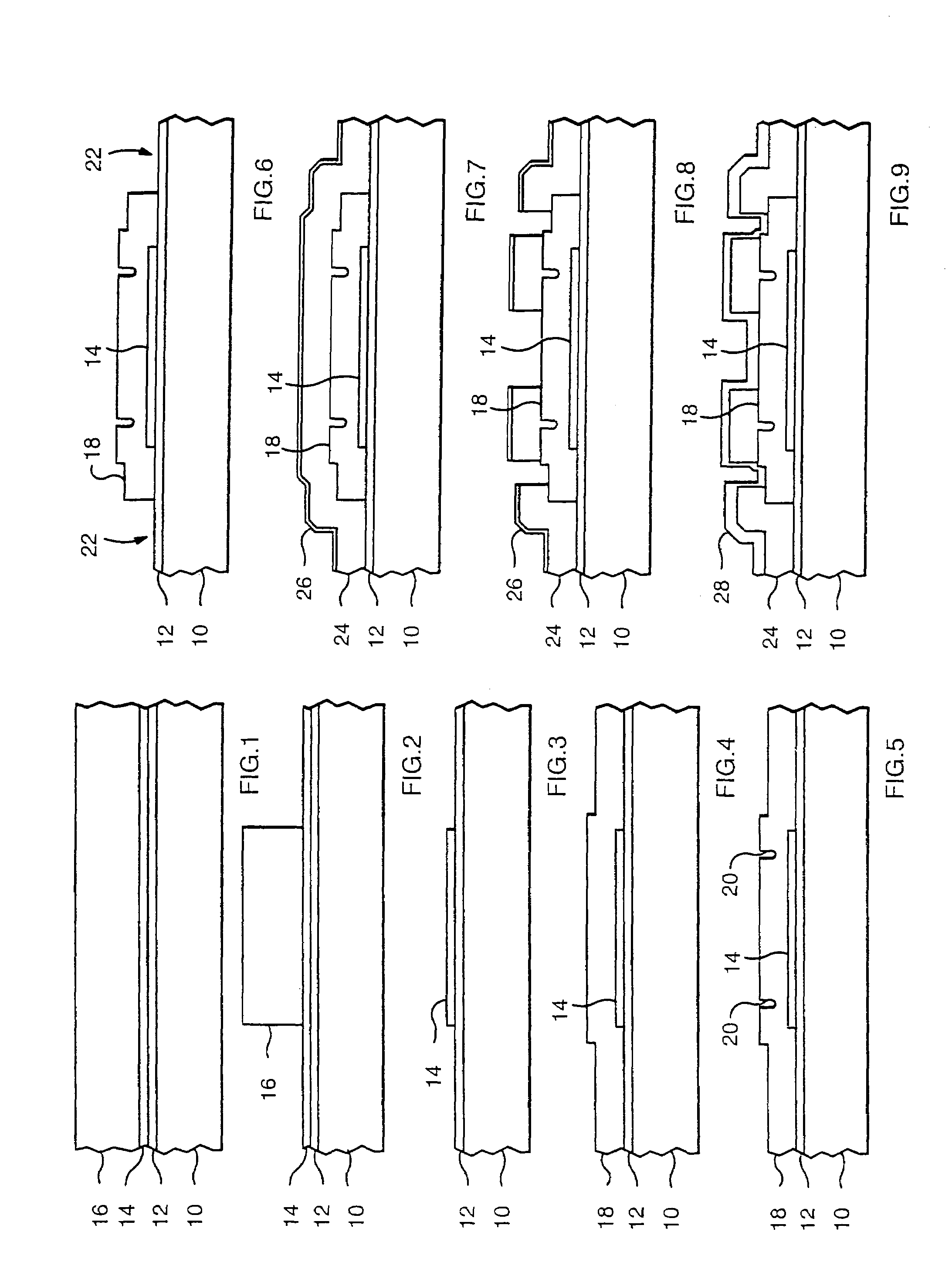
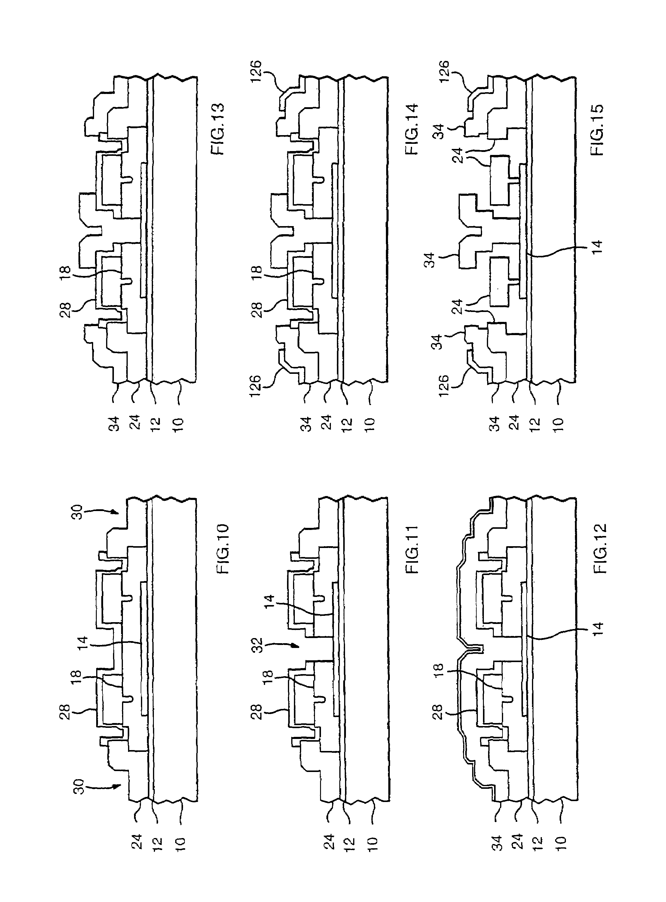
[0023]To assist with understanding the present invention, the general procedure for fabricating micromechanical devices using the MUMPs process is explained with reference to FIGS. 1–15.

[0024]The MUMPs process provides three-layers of conformal polysilicon that are etched to create a desired physical structure. The first layer, designated POLY 0, is coupled to a supporting wafer, and the second and third layers, POLY 1 and POLY 2, respectively, are mechanical layers that can be separated from underlying structure by the use of sacrificial layers that separate layers and are removed during the process.

[0025]The accompanying figures show a general process for building a micro-motor as provided by the MEMS Technology Applications Center, 3021 Cornwallis Road, Research Triangle Park, N.C.

[0026]The MUMPs process begins with a 100 mm n-type silicon wafer 10. The wafer surface is heavily doped with phosphorus in a standard diffusion furnace using POCI 3 as the dopant source. This reduces c...


PUM


Abstract

A unilateral in-plane thermal buckle-beam microelectrical mechanical actuator is formed on a planar substrate of semiconductor material, for example. The actuator includes first and second anchors secured to the substrate and a floating shuttle positioned movably parallel to the substrate. Symmetric first and second sets of elongated thermal half-beams are secured between the floating shuttle and the respective first and second anchors. The first and second anchors and the first and second sets of thermal half-beams are positioned along one side of the floating shuttle. The half-beams are formed of semiconductor material, such as polysilicon. A current source directs electrical current through the thermal half beams via the anchors to impart thermal expansion of the thermal half-beams and hence linear motion of the floating center beam generally parallel to the substrate. A floating cold beam connected between the shuttle and the substrate constrains and amplifies the motion of the shuttle in a predefined direction.

Description

CROSS REFERENCE TO RELATED APPLICATIONS[0001]This application is a continuation of application Ser. No. 10 / 036,810; filed Dec. 31, 2001 now U.S. Pat. No. 6,804,959 which is incorporated herein by reference in its entirety.FIELD OF THE INVENTION[0002]The present invention relates to microelectromechanical system (MEMS) actuators and, in particular, to thermal microelectromechanical system actuators that are activated by Joule heating.BACKGROUND OF THE INVENTION[0003]Microelectromechanical system (MEMS) actuators provide control of very small components that are formed on semiconductor substrates by conventional semiconductor (e.g., CMOS) fabrication processes. MEMS systems and actuators are sometimes referred to as micromachined systems-on-a-chip.[0004]One of the conventional MEMS actuators is the electrostatic actuator or comb drive. Commonly, such actuators include two comb structures that each have multiple comb fingers aligned in a plane parallel to a substrate. The fingers of th...

Claims


Application Information

Patent Timeline
Patent Type & Authority Patents(United States)
IPC IPC(8): F01B29/10B81B3/00F02G1/04F03G7/06
CPCB81B3/0024B81B3/0037F03G7/06F02G1/04B81B2201/032B81B2203/051B81B2203/0109
Inventor SINCLAIR, MICHAEL J.
Owner MICROSOFT TECH LICENSING LLC
Why Eureka
Try Eureka