Spatial light modulator with charge-pump pixel cell

a technology of charge-pumping and pixel cells, applied in the field of spatial light modulators, can solve the problems of large crts and lcds, the limitations of conventional crts and lcds become apparent, and the weight of large crts is very large and expensiv

Active Publication Date: 2006-03-14
TEXAS INSTR INC +1
View PDF16 Cites 46 Cited by
  • Summary
  • Abstract
  • Description
  • Claims
  • Application Information

AI Technical Summary

Benefits of technology

[0023]The present invention describes a novel pixel circuit design with area requirements comparable to that of a 1T1C DRAM-like pixel cell, but with the advantage of an output voltage swing of the full range allowed by the breakdown voltage of the pass transistor.

Problems solved by technology

But, as these requirements become more and more stringent, the limitations of conventional CRTs and LCDs become apparent.
But large CRTs are very bulky and expensive.
LCD panels are much lighter and thinner than CRTs, but are prohibitively expensive to manufacture in sizes competitive with large CRTs.
But, one disadvantage of LCDs is that they require a source of polarized light.
LCDs are therefore optically inefficient.
Without expensive polarization conversion optics, LCDs are limited to less than 50%-efficient use of an unpolarized light source.
This solution is bulkier and more expensive than a single-SLM solution, but allows the highest brightness levels for digital cinema and high-end video projection.
Designing high-voltage circuitry to individually control the pixels of an SLM is challenging.
Larger, HV-tolerant transistors may unacceptably reduce the cell area available for other critical cell components (such as the capacitor in a DRAM-type cell) or not fit in the cell at all.
A well-known drawback of the 1T1C DRAM circuit is the nonideal performance of the pass transistor.
So the transistors of the cell are themselves capable of tolerating Vc=Vdd, but the maximum actual Vc is limited to only Vdd−Vt due to the inherent properties of the 1T1C cell circuit.
This reduces the maximum available output Vc still further.
Many candidate circuit designs are impractical in a microdisplay due to the small pixel cell size.
However, the large design rules required for adequate spacing between PMOS and NMOS devices and their associated wells are impractical for small pixel sizes.
Alternatively, an SRAM pixel cell could be used, but this cell requires 6 transistors that also would likely not fit in the available pixel area.
Alternatively a PMOS transistor or diode could be added to the cell to ‘precharge’ the pixel cell high before writing it to a low value, but high-voltage PMOS devices or diodes also occupy an unacceptably large amount of area for small microdisplay pixels due to their associated well implants.
However, this would require even higher-voltage transistors than the high-voltage transistor in the cell.
Fabricating two types of high voltage (HV) transistors would increase cost and the cell would still not be able to use the highest-voltage transistors available.

Method used


Image

  • Spatial light modulator with charge-pump pixel cell
  • Spatial light modulator with charge-pump pixel cell
  • Spatial light modulator with charge-pump pixel cell

Examples


Embodiment Construction

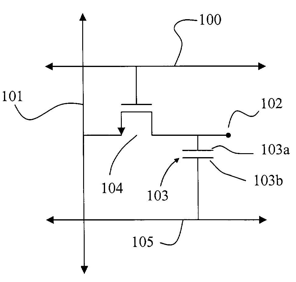
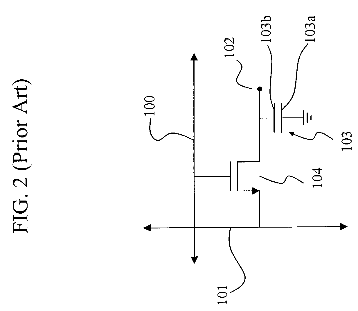
[0035]FIG. 2 is an illustration of a prior art DRAM cell circuit, whereas FIG. 3 is an illustration of a cell circuit of the present invention. As can be seen in both figures, each pixel contains a pass transistor 104 and a storage capacitor 103, as well as a wordline signal 100 for enabling access to a row of cells and a bitline signal 101 for reading and writing data to a column of cells. The cell's state is stored as a high or low voltage on the storage node 102. In a conventional DRAM illustrated in FIG. 2, first plate 103a of the storage capacitor is connected to the drain of the pass transistor. And the second plate node of the storage capacitor 103 is connected to a fixed supply voltage such as Vdd, Ground, or some intermediate supply voltage such as Vdd / 2 as is shown in FIG. 2. In the present invention illustrated in FIG. 3, the second capacitor plates of pixels in each row are connected to a ‘pump’ signal 105.

[0036]A simplified cross section of the circuit as implemented in...


PUM

PropertyMeasurementUnit
voltageaaaaaaaaaa
voltageaaaaaaaaaa
stored voltageaaaaaaaaaa

Abstract

A voltage storage cell circuit includes an access transistor and a storage capacitor, wherein the source of said access transistor is connected to a bitline, the gate of said access transistor is connected to a wordline, and wherein the drain of said access transistor is connected to a first plate of said storage capacitor forming a storage node, and wherein the second plate of said storage capacitor is connected to a pump signal. This arrangement allows for a novel pixel circuit design with area requirements comparable to that of a 1T1C DRAM-like pixel cell, but with the advantage of an output voltage swing of the full range allowed by the breakdown voltage of the pass transistor. A spatial light modulator such as a micromirror array can comprise such a voltage storage cell.

Description

[0001]This application claims the benefit of Provisional Application No. 60 / 347,736 filed Jan. 11, 2002.TECHNICAL FIELD OF THE INVENTION[0002]This invention relates generally to spatial light modulators used for display systems, and more particularly, to methods and apparatus for applying drive voltages to the pixels of such display systems.BACKGROUND OF THE INVENTION[0003]The well-known cathode ray tube (CRT) is widely used for television (TV) and computer displays. Other display technologies such as the transmissive liquid crystal display (LCD) panel are widely used in certain specialized applications such as displays for portable computers and video projectors.[0004]Market demand is continuously increasing for video displays with higher resolution, greater brightness, lower power, lighter weight, and more compact size. But, as these requirements become more and more stringent, the limitations of conventional CRTs and LCDs become apparent. Microdisplays the size of a silicon chip ...

Claims


Application Information

Patent Timeline
Patent Type & Authority Patents(United States)
IPC IPC(8): G09G3/36G02F1/1362G09G3/20G09G3/34G11C11/401G11C11/404G11C11/4074
CPCG09G3/34G11C11/404G11C11/401G02F1/136277G09G3/2018G09G3/346G09G2300/08G09G2310/0235G09G2310/0251G09G3/3648
Inventor RICHARDS, PETER W.
Owner TEXAS INSTR INC
Why Eureka
Try Eureka