Thin film forming device, method of forming a thin film, and self-light-emitting device

a technology of thin film and forming device, which is applied in the field of thin film forming device, self-lighting device, and method of forming thin film, which can solve the problem of material not passing

Inactive Publication Date: 2006-04-04
SEMICON ENERGY LAB CO LTD
View PDF52 Cites 16 Cited by
  • Summary
  • Abstract
  • Description
  • Claims
  • Application Information

AI Technical Summary

Benefits of technology

[0010]According to the present invention, the EL material is provided in a sample boat. By vaporizing and charging the EL material, it is discharged from an opening of the sample boat due to the vaporization, and, before it reaches a substrate, its direction of progress is controlled by the electric field generated by voltage applied to the mask, and thus, the location of deposition of the EL material can be controlled.
[0011]A plurality of masks may be used. For instance, an electric field is generated by voltages applied to a first mask and a second mask respectively, thereby controlling the direction of progress of the EL material and controlling the location where it is deposited.

Problems solved by technology

Here, there is a problem in that the EL material does not pass through the mask, but instead is deposited on the mask.

Method used


Image

  • Thin film forming device, method of forming a thin film, and self-light-emitting device
  • Thin film forming device, method of forming a thin film, and self-light-emitting device
  • Thin film forming device, method of forming a thin film, and self-light-emitting device

Examples


embodiment 1

(Embodiment 1)

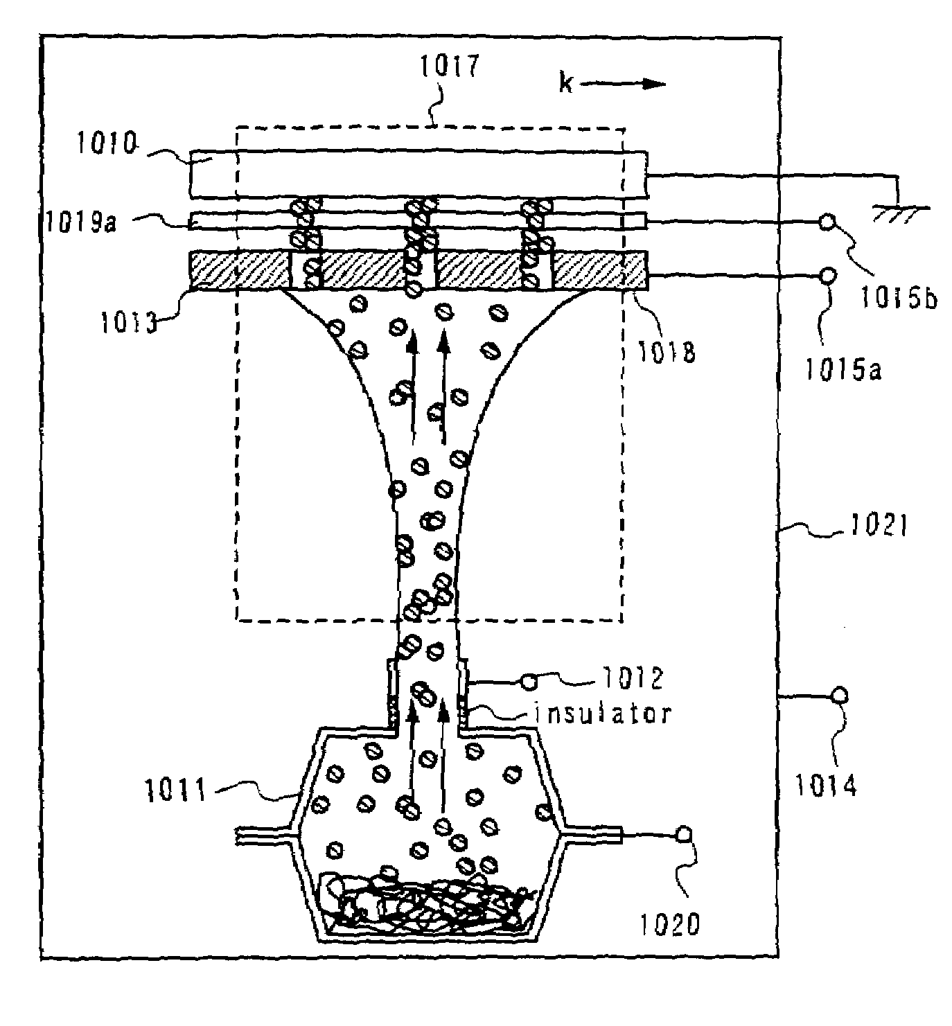
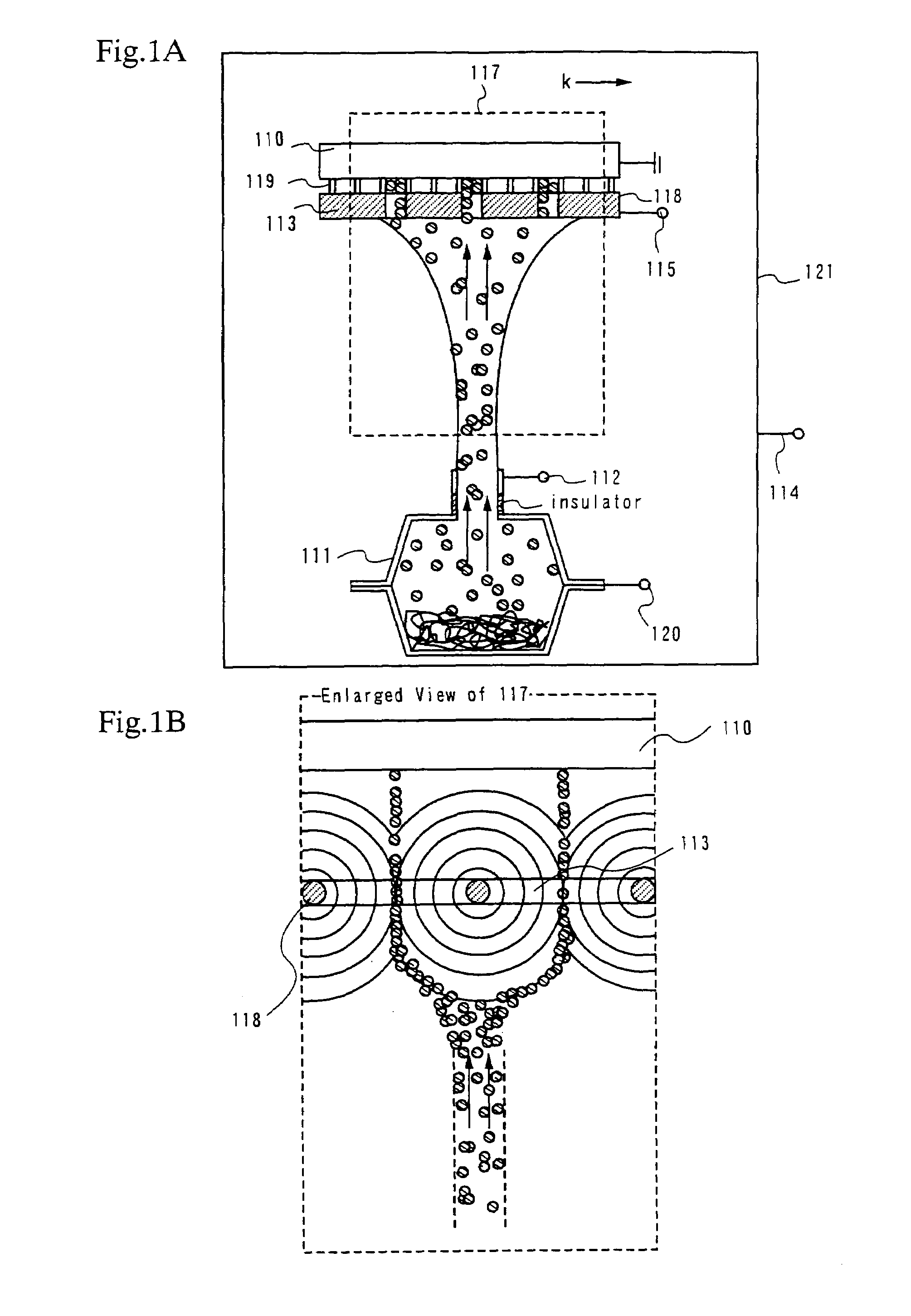
[0049]In this embodiment, a method of controlling an EL material vaporized in a sample boat (hereinafter referred to as an EL material in a vapor state) using an electric field and forming the film on a substrate is described with reference to FIGS. 1A and 1B.

[0050]In FIGS. 1A and 1B, a reference numeral 110 denotes a substrate. A sample boat 111 has a material for an EL layer.

[0051]It is to be noted that, when a red EL layer is to be formed, the sample boat 111 contains an EL material that emits red light (hereinafter referred to as a red EL material). When a green EL layer is to be formed, the sample boat 111 contains an EL material that emits green light (hereinafter referred to as a green EL material). When a blue EL layer is to be formed, the sample boat 111 contains an EL material that emits blue light (hereinafter referred to as a blue EL material).

[0052]It is to be noted that, in this embodiment, Alq as a host material with a red fluorescent pigment DCM doped t...

embodiment 2

(Embodiment 2)

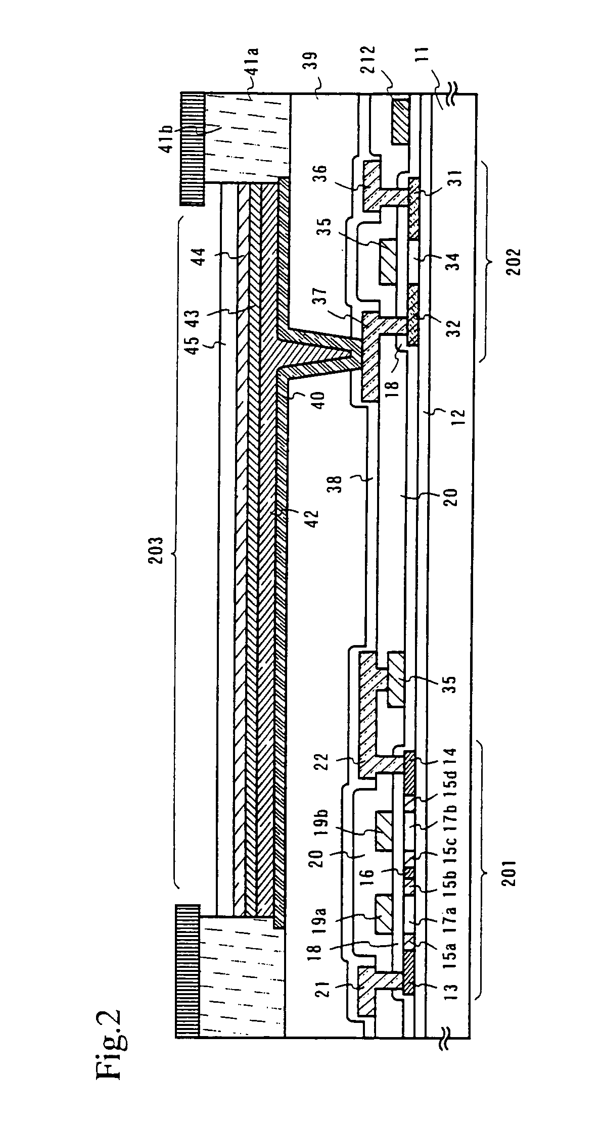
[0063]FIG. 2 is a sectional view of a pixel portion of an EL display device according to this embodiment. FIG. 3A is a top view of the pixel portion, and FIG. 3B illustrates its circuit structure. Actually, a plurality of pixels are arranged to be matrix-like to form a pixel portion (an image display portion). It is to be noted that FIG. 2 is a sectional view taken along the line A–A′ in FIG. 3A. Thus, since common numeralss are used in FIG. 2 and FIGS. 3A, 3B, and 3C, reference may be suitably made to the both drawings. Two pixels are illustrated in the top view of FIG. 3A, and the two pixels are of the same structure.

[0064]In FIG. 2, reference numerals 11 and 12 denote a substrate and an insulating film to be a base (hereinafter referred to as a base film), respectively. As the substrate 11, glass, glass ceramics, quartz, silicon, ceramics, metal, or plastic can be used.

[0065]Especially when a substrate containing movable ions or a conductive substrate is used, it is...

embodiment 3

(Embodiment 3)

[0108]Here, a method of forming a bank consisting of the bank a and the bank b illustrated in FIG. 3C is described. Both the bank a and the bank b are of positive type.

[0109]First, after a pixel electrode is formed, an organic resin film of melamine resin to be the bank a is formed. A dye is mixed in the melamine resin to make the organic resin film have a function as an antireflection film. These may be used after being dissolved in a solvent such as dimethylacetamide. It is to be noted that, in selecting the dye, it is necessary to select a dye having emission spectrum near the spectrum of light used in exposure.

[0110]Then, a polyimide film is laminated on the melamine resin film. Here, photosensitive polyimide or a novolac resin may be used instead of polyimide. This is to form the bank b.

[0111]It is to be noted that the organic resin film formed here has two layers. The organic resin film is then exposed to light to be patterned. As the developer for the patterning...


PUM

PropertyMeasurementUnit
thicknessaaaaaaaaaa
thicknessaaaaaaaaaa
thicknessaaaaaaaaaa

Abstract

Measure of forming an EL layer by selectively depositing through evaporation a material for forming the EL layer at a desired location is provided. When a material for forming an EL layer is deposited, a mask (113) is provided between a sample boat (111) and a substrate (110). By applying voltage to the mask (113), the direction of progress of the material for forming the EL layer is controlled to be selectively deposited at a desired location.

Description

[0001]This application is a divisional of U.S. application Ser. No. 09 / 798,608, filed on Mar. 2, 2001 now U.S. Pat. No. 6,699,739.BACKGROUND OF THE INVENTION[0002]1. Field of the Invention[0003]The present invention relates to a self-light-emitting device having an EL element formed on an insulator and structured to have an anode, a cathode, and a light-emitting organic material that provides electro luminescence (hereinafter referred to as an organic EL material) sandwiched therebetween, an electric apparatus having such a self-light-emitting device as a display unit (a display or a monitor), and a method of manufacturing thereof. It is to be noted that such an EL display device is sometimes referred to as an OLED (organic light emitting diode).[0004]2. Description of the Related Art[0005]These days, display devices using EL elements as self-light-emitting devices utilizing electro luminescence of a light-emitting organic material (EL display devices) are actively developed. Since ...

Claims


Application Information

Patent Timeline
Patent Type & Authority Patents(United States)
IPC IPC(8): H01L21/00H05B33/10C23C14/04H01L27/32H01L51/00H01L51/30H01L51/40
CPCC23C14/042H01L51/001H01L51/0077H01L51/0011H01L27/32H01L27/3211H01L27/3244H01L27/3281Y10S438/942H01L51/0065H01L51/0078H01L51/0085H01L51/0087H01L51/56H10K59/35H10K59/00H10K59/17H10K59/12H10K71/164H10K71/166H10K85/653H10K85/311H10K85/30H10K85/346H10K85/342H10K71/00F24F13/0209F24F13/0281F24F13/0245F24F13/068F24F7/10
Inventor YAMAZAKI, SHUNPEIHIROKI, MASAAKIISHIMARU, NORIKO
Owner SEMICON ENERGY LAB CO LTD
Why Eureka
Try Eureka