Electron impact ion source

a technology of ion beams and ion beams, applied in the field of ion sources, can solve the problems of high current (>1 ma) ion beams at low (5 kev) energy, increase beam diameter and beam angular, and beam loss

Inactive Publication Date: 2006-04-04
SEMEQUIP
View PDF22 Cites 11 Cited by
  • Summary
  • Abstract
  • Description
  • Claims
  • Application Information

AI Technical Summary

Benefits of technology

[0009]Ionizing electron beams generated external to the ionization chamber, thereby extending the emitter lifetime.
[0012]Use of a deceleration lens to adjust the ionization energy of the electron beam, substantially without affecting electron beam generation and deflection.

Problems solved by technology

The production of beams possessing these characteristics imposes severe constraints on the beam transport optics of the implanter, and the commonplace use of large-emittance plasma-based ion sources often results in increased beam diameter and beam angular divergence, causing beam loss during transport due to vignetting of the beam by the various apertures present within the beam line of the implanter.
Currently, the generation of high current (>1 mA) ion beams at low (<5 keV) energy is problematic in serial implanters, such that wafer throughput is unacceptably low for certain low-energy implants (for example, in the creation of source and drain structures in leading-edge CMOS processes).
Similar transport problems also exist for batch implanters (processing many wafers mounted on a spinning disk) at the low beam energies of <5 keV per ion.
Arc-discharge plasma sources currently in use have poor emittance, and therefore severely limit the ability of ion implanters to produce well-focused, collimated, and controllable ion beams.

Method used


Image

  • Electron impact ion source
  • Electron impact ion source
  • Electron impact ion source

Examples


Embodiment Construction

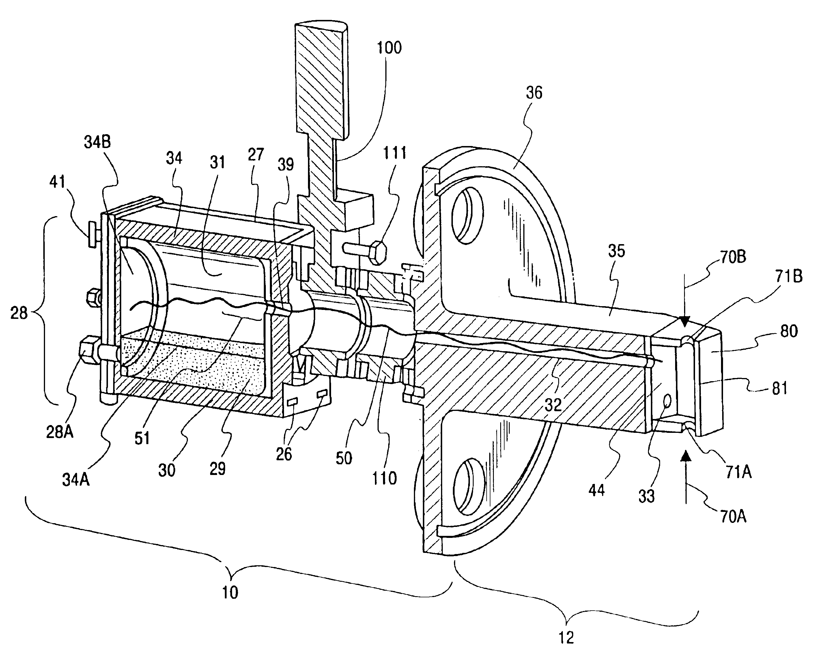
[0020]The ion source which forms a part of the ion implantation system in accordance with the present invention is an electron impact ionization source. FIG. 1 is a cross-sectional schematic diagram of the ion source in accordance with the present invention which illustrates the construction and the functionality of the components which make up the ion source 10. The cross section is cut along a plane which contains the direction of propagation of the ion beam, separating the ion source in two halves. The ion source 10 includes a vaporizer 28 and a beam forming region 12 joined together by at a mounting flange 36. The ion source 10 is made to interface to an evacuated vacuum chamber of an ion implanter or other process tool by way of the mounting flange 36. Thus, the portion of the ion source 10 to the right of the flange 36 in FIG. 1 is at high vacuum (pressure −4 Torr). Gaseous material is introduced into an ionization chamber 44 where the gas molecules are ionized by electron imp...


PUM


Abstract

An ion source configured for integration into both existing ion implanters used in semiconductor manufacturing and emerging ion implantation platforms. The ion source in accordance with the present invention includes the following features, all of which depart from the prior art to produce a well-focused, collimated and controllable ion beam. These features include: ionizing electron beams generated external to the ionization chamber, thereby extending the emitter lifetime; 90 degree magnetic deflection of electron beams such that no line-of-sight exists between the emitter and the process gas load, and the emitter is protected from bombardment by energetic charged particles; two opposed electron beams which can be operated simultaneously or separately; and use of a deceleration lens to adjust the final energy of the electron beam, substantially without affecting electron beam generation and deflection.

Description

CROSS-REFERENCE TO RELATED APPLICATIONS[0001]This is a continuation of prior application Ser. No. 10 / 183,768, filed Jun. 26, 2002, now U.S. Pat. No. 6,686,595, which is hereby incorporated herein by reference in its entirety.BACKGROUND OF THE INVENTION[0002]1. Field of the Invention[0003]The present invention relates to an ion source and more particularly to an electron impact ion source.[0004]2. Description of the Prior Art[0005]Ion implantation has been a key technology in semiconductor device manufacturing for more than twenty years, and is currently used to fabricate the p-n junctions in transistors, particularly in CMOS devices, such as memory and logic chips. By creating positively-charged ions containing various dopant elements, such as, 75As, 11B, 115In, 31P, or 121Sb, required for fabricating the transistors in, for example, silicon substrates, known ion implanters can selectively control both the energy (hence implantation depth) and ion current (hence dose) of ions introd...

Claims


Application Information

Patent Timeline
Patent Type & Authority Patents(United States)
IPC IPC(8): H01J7/24H01J27/20
CPCH01J27/20H01J37/08H01J37/3171H01L29/66575H01L21/823814H01L21/823842H01L27/092H01L21/26513H01J2237/061H01J2237/082H01J2237/304H01L21/3215H01L21/67213H01L21/2658
Inventor HORSKY, THOMAS N.
Owner SEMEQUIP
Why Eureka
Try Eureka