Method for forming damascene structure utilizing planarizing material coupled with diffusion barrier material

a damascene and diffusion barrier technology, applied in the manufacture of cable/conductor, basic electric elements, electric apparatus, etc., can solve the problems of poisoning of the line imaging layer, and much worse poisoning problems

Active Publication Date: 2006-04-18
GLOBALFOUNDRIES US INC
View PDF17 Cites 71 Cited by
  • Summary
  • Abstract
  • Description
  • Claims
  • Application Information

AI Technical Summary

Benefits of technology

[0019]This invention is based on using the combination of a planarizing layer followed by a barrier layer which prevents photoresist poisoning. The use of a planarizing layer circumvents filling an etched pattern such as a deep aspect ratio trench. The preferred planarizing layer has superior planarization performance as well as superior thermal stability compared to many typical resist or arc materials used conventionally to fill vias during dual damascene patterning. These lead to improved manufacturability of fine patterns, as well as the ability to deposit an LTO film at temperatures suitable to achieve good barrier properties. The barrier layer deposited on top of the planarizing layer should be chemically stable, mechanically sound, relatively defect free, should not damage the planarizing layer, and should act as a barrier to photoresist poisoning.

Problems solved by technology

All of these methods are fraught with problems.
With the via-first approach, the use of photoresist layers on dielectric layers often results in “poisoning” of the line imaging layer which is done after vias are fully or partially etched into the dielectric.
The poisoning problem appears to be much worse when the dielectric layer is a low-k insulator applied using chemical vapor deposition (CVD), as compared to silicate glass dielectric layers.
Attempts to solve the poisoning problems have been incomplete.
However, such resist materials compromise imaging resolution and decrease lithographic process window.
However, such modifications may adversely affect the dielectric constant and other characteristics of the insulating materials.
Also, certain underlying dielectric materials such as dielectric barrier caps on underlying Cu levels preferably contain nitrogen and hydrogen, and can be a source of poisoning that might not be easily remedied.
Removing the nitrogen compromises the barrier properties, and removing the hydrogen raises the dielectric constant to unacceptable levels.
Even when a spin-on glass (SOG) layer was added between the planarizing and imaging layers (presumably for resist budget during etch), poisoning still occurred through this SOG layer.
Since it is difficult to deposit materials in high-aspect ratio vias, this approach may not be extendable to future technologies.
Defects in thin regions of this liner may allow poisoning gases to pass through, and even with low statistical occurrence may cause an unacceptable level of defective patterns in the line imaging layer.
These methods are more complex and can be difficult for RIE manufacturing, because the RIE must be able to etch the dielectric with high selectively to the hardmask materials.
That in turn may constrain the conditions under which the RIE may operate, and hence may compromise the ability to achieve the desired patterning control in the dielectric film.
However, in the case of Si-containing dielectric materials such as SICOH, it is difficult to obtain high etch selectivity to any common hardmask materials, including metal nitrides.
The line-first approach suffers from the difficulty of printing vias inside lines, especially at small dimensions.
It becomes difficult or impossible to define a photolithographic dose and focus process window that can image simultaneously all vias in all line pattern situations.
As the via becomes ever smaller in size, it becomes ever more difficult to expose and develop out a via image through the extra thickness of resist that fills in, and becomes planar over, the line structure.
Moreover, resist poisoning may continue to be a problem with this approach, as the already-etched line trenches expose the low-k dielectric to the via imaging layer, allowing amines, if present, to and poison this imaging layer.
Photoresist poisoning is a problem well known in the industry.
Others skilled in the art have been unsuccessful in attempts to produce a barrier layer which prevents poisoning but does not damage planarizing material during its deposition.
It is believed to be ever more difficult to find a material that meets all these requirements.
There is currently not a known strip process for this material that would be compatible with patterned low-k dielectrics.
In general, circumventing the phenomenon of resist poisoning has placed significant constraints on other elements in the multilevel damascene integration, especially for low-k insulators, that were not the case in previous generations; these constraints are not desired and represent disadvantages.
As in the Higashi et al. paper, limitations are placed on choices that do not result in poisoning for the Cu barrier cap, the interlevel dielectric material itself, the etching and stripping chemistries used, the need for caps over the interlevel dielectric, and the choice of the resist imaging layer material itself.

Method used


Image

  • Method for forming damascene structure utilizing planarizing material coupled with diffusion barrier material
  • Method for forming damascene structure utilizing planarizing material coupled with diffusion barrier material
  • Method for forming damascene structure utilizing planarizing material coupled with diffusion barrier material

Examples


Embodiment Construction

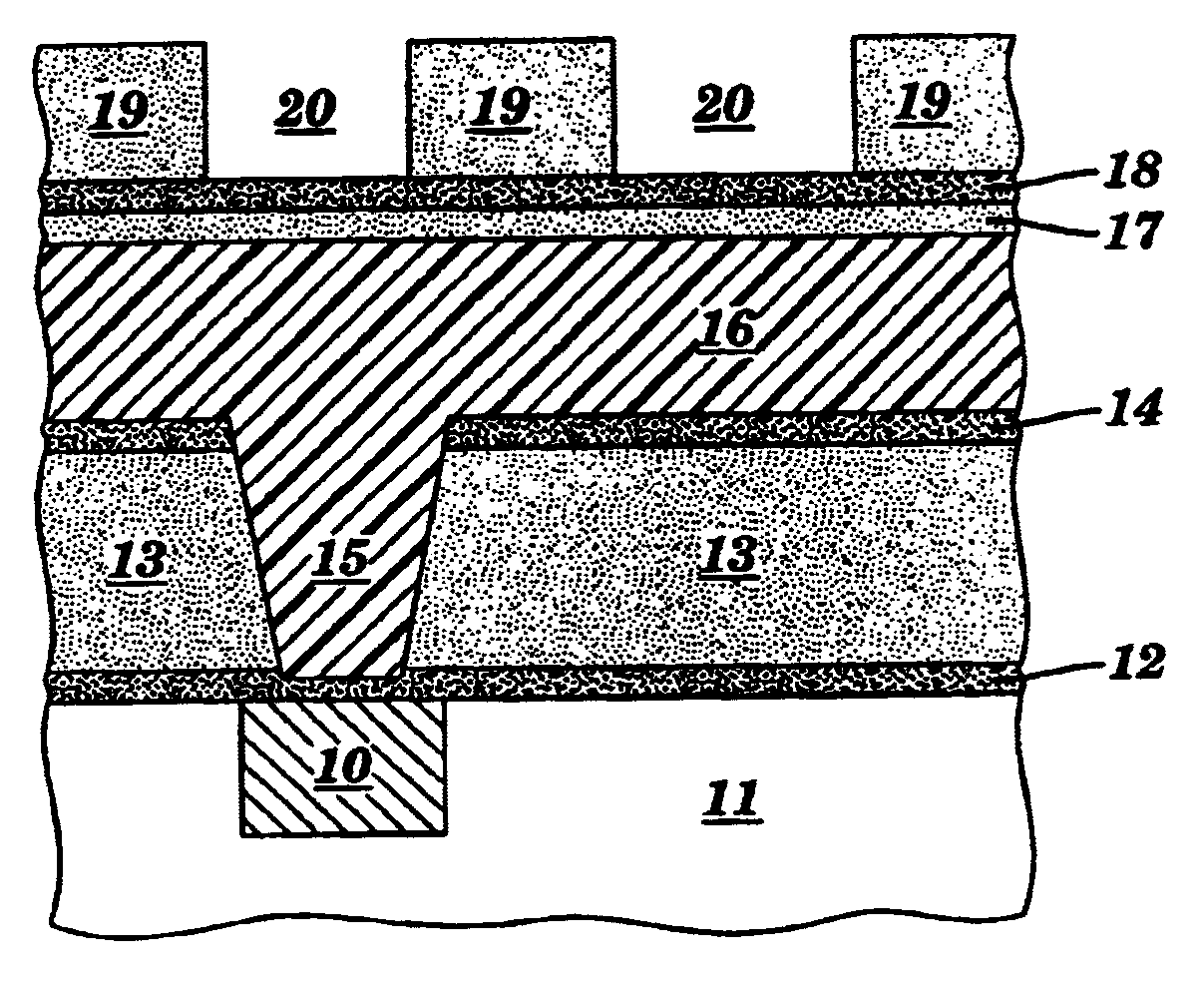
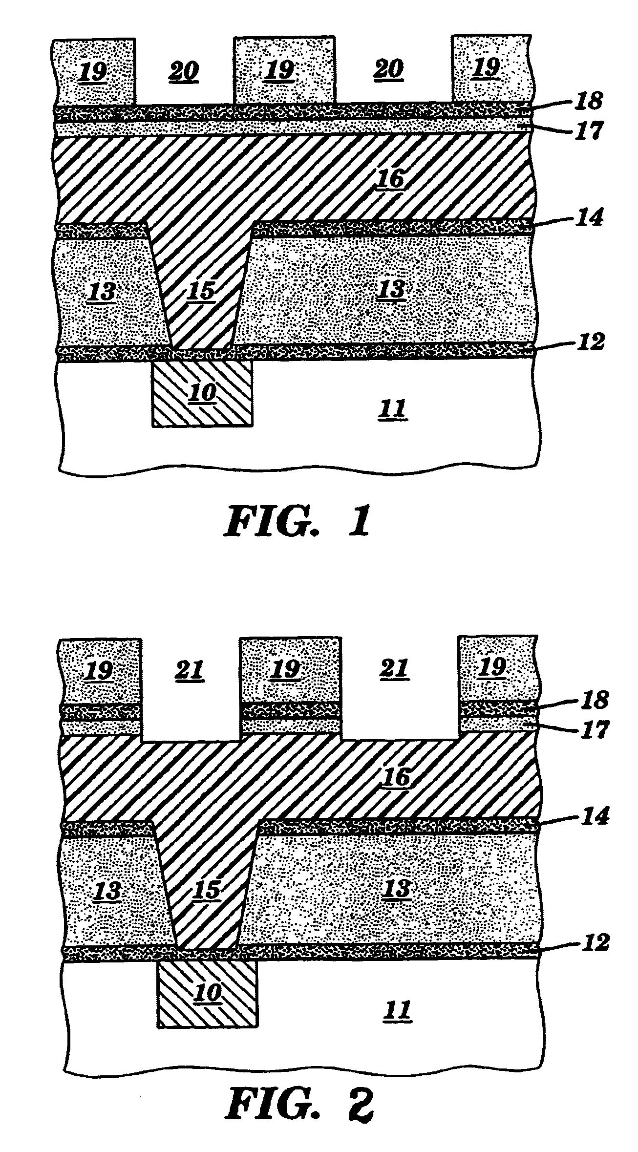
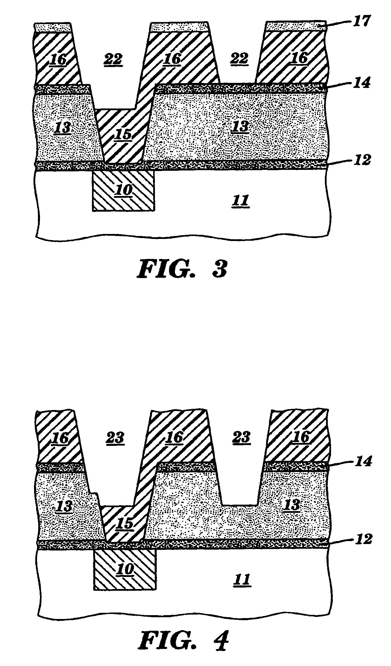
[0017]The invention will now be described by reference to the accompanying figures. In the figures, various aspects of the structures have been shown and schematically represented in a simplified manner to more clearly describe and illustrate the invention. For example, the figures are not intended to be to scale. In addition, the vertical cross-sections of some of the various aspects of the structures are illustrated as being rectangular in shape. Those skilled in the art will appreciate, however, that with practical structures these aspects will most likely incorporate more tapered features. Moreover, the invention is not limited to constructions of any particular shape.

[0018]The problem of poisoning described above is solved by depositing a planarizing film on a patterned wafer and then depositing a barrier layer, preferably a low temperature oxide (LTO) film, on top of the planarizing film. Conventional lithographic patterning is performed on top of the LTO film. This invention ...


PUM

PropertyMeasurementUnit
dielectric constantaaaaaaaaaa
temperatureaaaaaaaaaa

Abstract

This invention relates to the manufacture of dual damascene interconnect structures in integrated circuit devices. Specifically, a method is disclosed for forming a single or dual damascene structure in a low-k dielectric thin film utilizing a planarizing material and a diffusion barrier material. In a preferred dual damascene embodiment of this method, the vias are formed first in the dielectric material, then the planarizing material is deposited in the vias and on the dielectric material, and the barrier material is deposited on the planarizing material. The trenches are then formed lithographically in the imaging material, etched through the barrier material into the planarizing material, and the trench pattern is transferred to the dielectric material. During and following the course of these etch steps, the imaging, barrier and planarizing materials are removed. The resultant dual damascene structure may then be metallized. With this method, the problem of photoresist poisoning by the interlevel dielectric material is alleviated.

Description

BACKGROUND OF INVENTION[0001]This invention relates generally to the manufacture of integrated circuit devices, and more specifically, to the manufacture of single and dual damascene interconnect structures in integrated circuit devices.[0002]Several basic methods for forming a dual damascene structure have been developed. These include the via-first approach, the line-first approach, and various hardmask schemes. All of these methods are fraught with problems.[0003]With the via-first approach, the use of photoresist layers on dielectric layers often results in “poisoning” of the line imaging layer which is done after vias are fully or partially etched into the dielectric. This is the case even when bottom anti-reflective coatings are used to fill the vias temporarily, so as to provide a planar surface for the line imaging layer. The source of this poisoning is not clearly understood, but it is thought to be due to absorption and / or generation and liberation of amine compounds from ...

Claims


Application Information

Patent Timeline
Patent Type & Authority Patents(United States)
IPC IPC(8): H01L21/302H01L21/768
CPCH01L21/31144H01L21/76808H01L21/76804H01L21/768
Inventor WILLE, WILLIAM C.EDELSTEIN, DANIEL C.COTE, WILLIAM J.BIOLSI, PETER E.FRITCHE, JOHNUPHAM, ALLAN W.
Owner GLOBALFOUNDRIES US INC
Why Eureka
Try Eureka