Apparatus for fabricating a III-V nitride film and a method for fabricating the same

a technology of nitride film and nitride film, which is applied in the direction of crystal growth process, polycrystalline material growth, chemically reactive gas, etc., can solve the problem that the hvpe method cannot achieve good and stable properties, the aln film with poor crystallinity cannot be used for opto-electronic device substrates, and the hvpe method is not suitable for the above method. problem, to achieve the effect of reducing the cost of fabrica

Inactive Publication Date: 2006-04-25
NGK INSULATORS LTD
View PDF20 Cites 24 Cited by
  • Summary
  • Abstract
  • Description
  • Claims
  • Application Information

AI Technical Summary

Benefits of technology

[0017]In the first fabricating apparatus, the whole of the reactor may be made of aluminum nitride material in fabricating a III–V nitride film including at least Al element. Moreover, the reactor body may be made of silicon oxide and an AlN film may be coated on the inner surface of the reactor body to complete the reactor to be used in the present invention. In both cases, the reactor is not corroded by the AlCl gas. In the former case, the AlN film can be fabricated by a thermal CVD method. Therefore, the reactor body c...

Problems solved by technology

It is confirmed, however, that the AlN film with good and stable properties cannot be fabricated using the above conventional HVPE method.
However, the silicon oxide-based material is likely to be corroded by an aluminum chloride gas generated through the reaction of an aluminum metallic material and a chloride-based gas to form pinholes in the reactor.
Such a poor crystallinity AlN film can not be used for an opto-electronic device substrate.
Moreover, if the pinholes are formed in the reactor through the corrosion of the AlCl gas...

Method used


Image

  • Apparatus for fabricating a III-V nitride film and a method for fabricating the same
  • Apparatus for fabricating a III-V nitride film and a method for fabricating the same
  • Apparatus for fabricating a III-V nitride film and a method for fabricating the same

Examples


Embodiment Construction

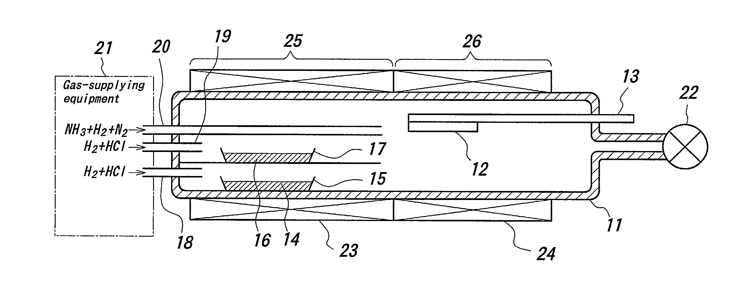
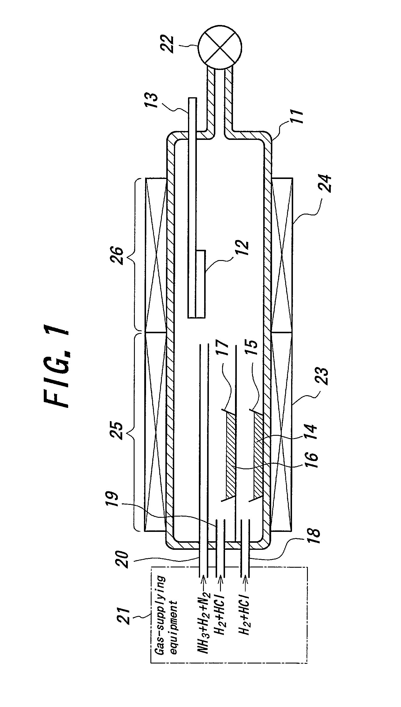
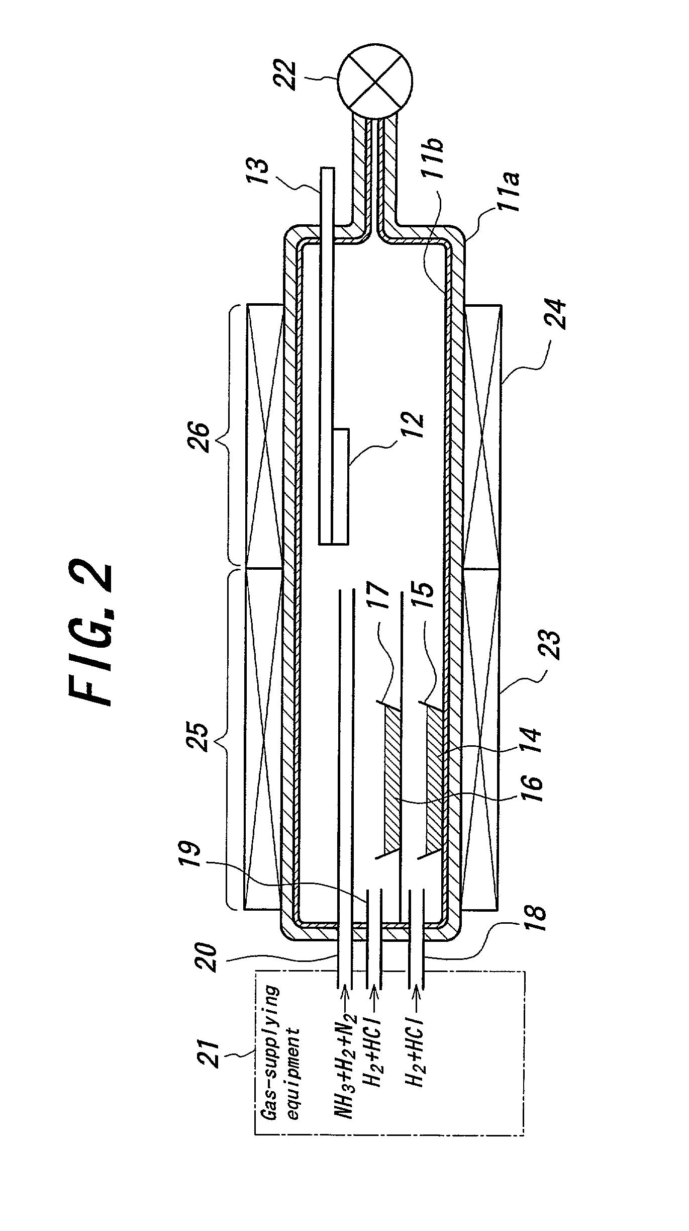
[0038]FIG. 1 is a structural view showing a first embodiment of the first fabricating apparatus of the present invention. In this embodiment, the whole of the reactor 11 is made of an aluminum nitride material not to be corroded by an AlCl gas. Herein, the wall thickness of the reactor 11 is exaggerated. The aluminum nitride material has a hexagonal or a cubic crystal structure, and may incorporate other elements up to 10% or so as impurities or additives.

[0039]Also, in this embodiment, an AlGaN film will be fabricated.

[0040]In the reactor 11 are arranged a susceptor 13 to hold a sapphire substrate 12 horizontally, a boat 15 to hold an aluminum metallic material 14 and a boat 17 to hold a gallium metallic material 16. In this embodiment, although the sapphire substrate 12 is held downward, it may be upward.

[0041]In this embodiment, a GaN underfilm is formed on the sapphire substrate 12 beforehand to complete an epitaxial growth substrate 12. For the sake of this, the boats 15 and 17...


PUM

PropertyMeasurementUnit
Pressureaaaaaaaaaa
Concentrationaaaaaaaaaa
Corrosion propertiesaaaaaaaaaa

Abstract

A hydrogen chloride gas and an ammonia gas are introduced with a carrier gas into a reactor in which a substrate and at least an aluminum metallic material through conduits. Then, the hydrogen gas and the ammonia gas are heated by heaters, and thus, a III–V nitride film including at least Al element is epitaxially grown on the substrate by using a Hydride Vapor Phase Epitaxy method.
The whole of the reactor is made of an aluminum nitride material which does not suffer from the corrosion of an aluminum chloride gas generated by the reaction of an aluminum metallic material with a hydrogen chloride gas.

Description

BACKGROUND OF THE INVENTION[0001]1. Field of the Invention[0002]This invention relates to an apparatus and a method for epitaxial growth of a III–V nitride film including at least Al element on a substrate by using a Hydride Vapor Phase Epitaxy (HVPE) method.[0003]2. Related Art Statement[0004]In opto-electronic device such as light-emitting diodes and laser diodes, it is proposed that a III–V nitride film having a composition of AlxGayInzN (X+Y+Z=1) including at least Al element is epitaxially grown on a given substrate. For example, it is described in “J. Appl. Phys., 68, No. 7 (1999)”, from pp774 onward that a GaN film is epitaxially grown on a sapphire substrate.[0005]In this method, a Ga metallic material is charged into a reactor in which a sapphire substrate having a GaN film on its surface is held, and a hydrochloric gas is also introduced into the reactor to generate a gallium chloride gas. Then, the gallium chloride gas and an ammonia gas are reacted with each other to dep...

Claims


Application Information

Patent Timeline
IPC IPC(8): C30B25/08C30B25/02C30B25/16C30B29/38H01L21/20H01L21/205
CPCC30B25/02C30B29/403C30B29/406Y10T117/10Y10T117/1008H01L21/20
Inventor SHIBATA, TOMOHIKOASAI, KEIICHIROTANAKA, MITSUHIRO
Owner NGK INSULATORS LTD
Why Eureka
Try Eureka