Means of seeding and metallizing polyimide

a technology of metallizing polyimide and seeding, which is applied in the direction of liquid/solution decomposition chemical coating, transportation and packaging, nuclear engineering, etc., can solve the problems of poor adhesion of metal layers (or discrete lines and features), unattractive practice, and high cost of deposition process, so as to achieve enhanced adhesion between metals

Inactive Publication Date: 2006-04-25
IBM CORP
View PDF10 Cites 27 Cited by
  • Summary
  • Abstract
  • Description
  • Claims
  • Application Information

AI Technical Summary

Benefits of technology

[0010]It is an object of the method of the present invention to render the surface of a polyimide used in the standard electronic packaging applica

Problems solved by technology

However the adhesion of metal layers (or discrete lines and features) is typically poor for most methods of metallizing the polyimide without an adhesive layer.
This practice is unattractive for two major reasons: (1) deposition processes use costly high vacuum processes having additional process steps (e.g. resist coating, lithography, resist developing,

Method used


Image

  • Means of seeding and metallizing polyimide
  • Means of seeding and metallizing polyimide
  • Means of seeding and metallizing polyimide

Examples


example 1

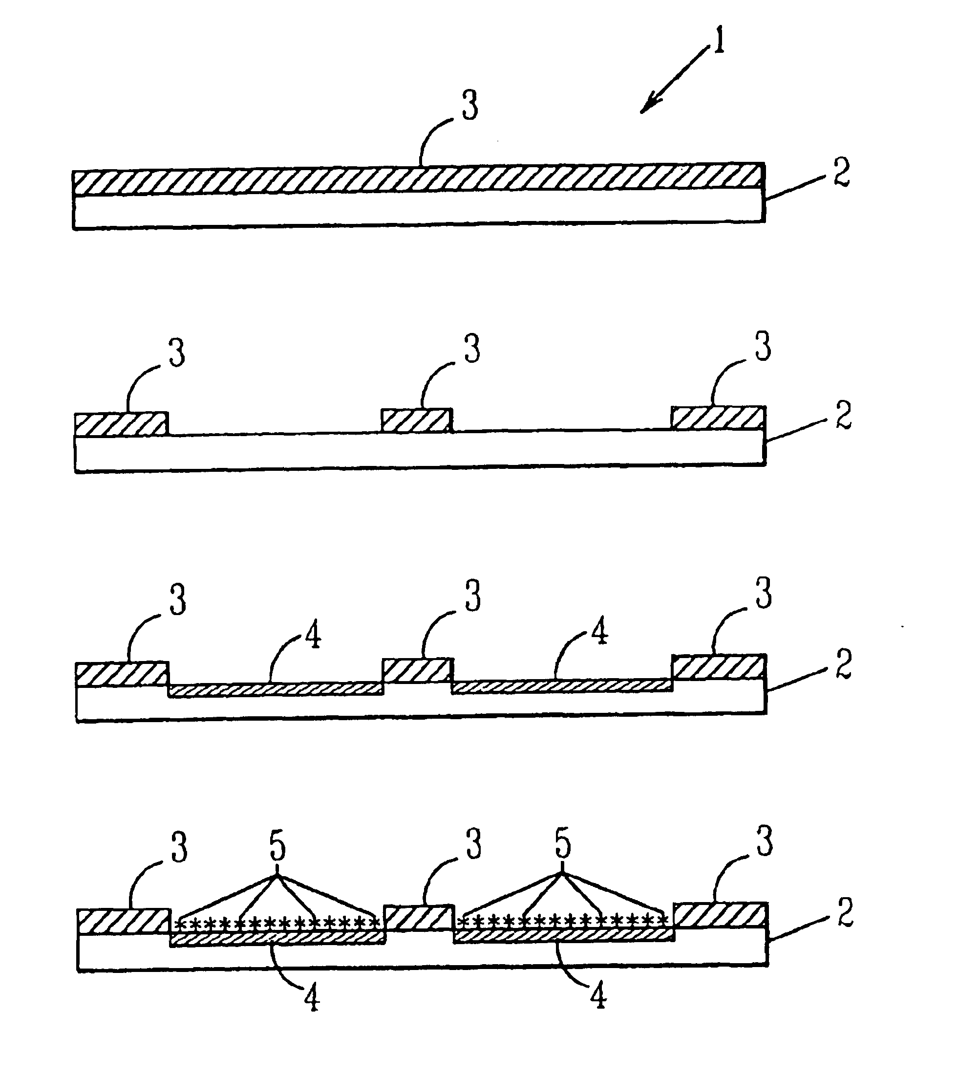
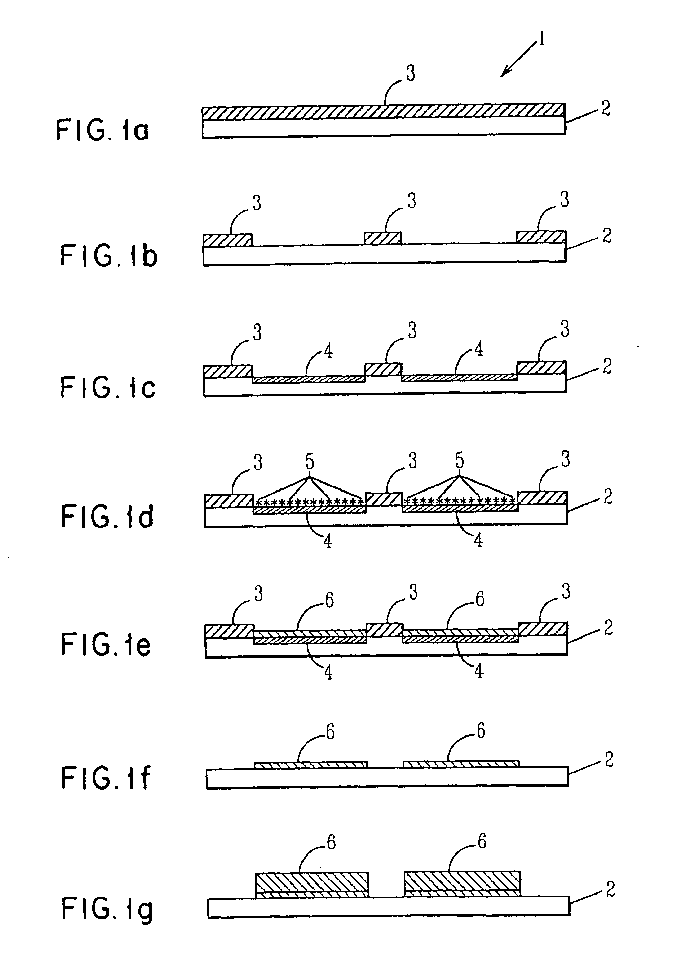
[0068]Samples of an imide polymer designated Polyimide 2525 having a thickness of 0.001 (1 micron) cm were dried at low temperature to 69 weight percent solids at 94% amic acid. Each polyimide substrate (2) was coated with a layer (3) (between 1 and 10 microns of a blend of poly(methymethacrylate) and Tinuvin 328 ultra violet absorbing dye. FIG. 1(a) shows the resist coated polyimide product (1).

[0069]The composite film (1) (resist / polyimide) was subjected to a 308 nm laser through a mask atop the polyimide. The poly(methymethacrylate) resist (3) was removed from areas where Cu deposition was desired. FIG. 1(b) shows the laser pattern after laser ablation has occurred.

[0070]According to the preferred embodiment, the exposed polyimide surface was exposed a 0.4M sodium hydroxide solution by immersing the work piece into the solution. FIG. 1(c) depicts the work piece after hydrolysis has occurred and shows the layer of hydrolysate reaction product (4) in place on the polyimide.

[0071]Th...

example 2

[0076]The process described in Example 1 was duplicated with the exception that poly(alpha-methylstyrene) was substituted for the poly(methylmethacrylate). The resultant product has the same beneficial properties as the product prepared in Example 1.

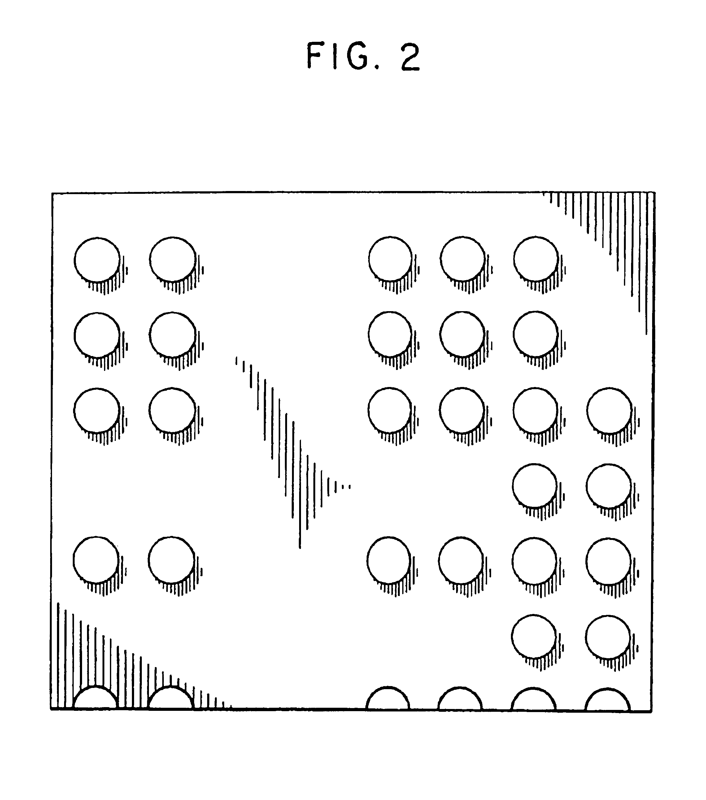
[0077]The process disclosed above has been implemented successfully with readily available materials in a bench top environment and is readily adaptable to manufacturing scale batch processing. FIG. 2 shows an optical micrograph of a pattern built using the method described above.


PUM

PropertyMeasurementUnit
Nanoscale particle sizeaaaaaaaaaa
Thicknessaaaaaaaaaa

Abstract

A method to selectively metallize polyimide with an all-electroless process.

Description

[0001]This application is a continuation of application Ser. No. 08 / 384,065, filed Feb. 6, 1995, now abandoned.TECHNICAL FIELD[0002]The present invention relates to a method for selectively metallizing the surface of a polyimide film using an all electroless process. The deposition scheme allows enhanced adhesion between the metal, usually copper, and the polyimide substrate. Specific type resist systems are used to obtain selective plating.PRIOR ART[0003]The use of polymeric dielectrics such as polyimides, polysiloxanes, silicones, cyclobutadienes and other high temperature polymers like polyphenylquinoxaline in semi-conductor technology especially electronic packaging applications is well known. Particularly useful among the aforementioned compositions is polyimide.[0004]Metallization of polyimide is of great importance to various low-end and high-end packages such as, MCM-L, flex circuits, etc. However the adhesion of metal layers (or discrete lines and features) is typically poo...

Claims


Application Information

Patent Timeline
IPC IPC(8): H05H1/00B05D3/00B05D5/12
CPCC23C18/1605C23C18/1692C23C18/2006C23C18/208C23C18/22C23C18/30C23C18/31H05K3/184C23C18/1641H05K2203/095H05K1/0346H05K3/0032H05K3/381H05K2203/0793H05K2203/083
Inventor DOANY, FUAD E.MARINO, JEFFREY R.SAMBUCETTI, CARLOS J.SARAF, RAVI F.
Owner IBM CORP
Why Eureka
Try Eureka