Reducing the effect of simultaneous switching noise

a technology of simultaneous switching and noise reduction, applied in pulse manipulation, pulse technique, instruments, etc., can solve the problems of system error, increased noise, increased noise, etc., and achieve the effect of reducing the number of i/o buffer circuits connected, simple and inexpensive implementation, and reducing the impact of data delay

Inactive Publication Date: 2006-05-09
AVAGO TECH WIRELESS IP SINGAPORE PTE
View PDF13 Cites 13 Cited by
  • Summary
  • Abstract
  • Description
  • Claims
  • Application Information

AI Technical Summary

Benefits of technology

[0018]It will be seen that by monitoring the number of simultaneous H-L transitions which occur at any one time in the data applied to the buffer inputs, and by inverting the data when the number exceeds half the number of data lines, the present invention enables the number of I / O buffer circuits connected to VSS pins to be increased or doubled without violating the SSO rules. For example, if N buffers in an IC were switching simultaneously and the SSO number was N / 4, then four VSS pins would be required to avoid high ground bounce that may cause false pulses being transmitted to the receiving IC. By using the present invention only N / 2 VSS pins would be required since only up to one half of the data lines are allowed to switch from high to low simultaneously.
[0019]The present invention has little impact on data delay and is simple and inexpensive to implement. It requires only a few extra logic gates to be added to an IC in order to double the maximum number of buffers that can be connected to a set of VSS pins. The technique has no impact on the data transfer rate and only introduces a minimal latency of 0.5 clock pulse in the data path. It reduces the effect of simultaneous switching noise based on existing SSO analysis for the buffer / package combination used and helps reduce the power consumption of the output buffers by allowing only less than half the buffers to switch at any transition.
[0020]In pad-limited designs, the present invention can have a great advantage particularly when using high current drivers with low SSO numbers. For example, if sixty-four buffers were used to transfer data and the SSO number was eight then a minimum of eight ground pins would be required to prevent ground bounce problems. By using the present invention the SSO can be doubled to sixteen thus reducing the VSS requirements to four pins only. However, this does require an extra pin for the flag signal resulting in a saving of seven pins. Larger savings in VSS pins can be achieved in designs with a larger number of I / O buffers.
[0021]The objects, features and advantages of the present invention include providing an improved method and apparatus for integrated circuit input / output switching that may (i) increase the number of buffers connected to a VDD / VSS pair, (ii) cause little impact on data delay, (iii) be inexpensive to implement, (iv) require only a few extra logic gates to be added to an IC, (v) reduce the effect of simultaneous switching noise, and / or (vi) reduce the power consumption of the buffers.

Problems solved by technology

Many I / O switching buffers simultaneously performing the H-L transition can give rise to what is known as ground bounce (i.e., a temporary rise in the ground voltage) and thus increased noise.
Several I / O switching buffers simultaneously performing the L-H transition can give rise to what is known as a power droop and thus increased noise.
Such false pulses are passed via the transmission lines to the receiving IC which treats the false pulses as true pulses, resulting in a system error.
The analysis, in turn, results either in a limitation in the number of pins that can be used for transferring data from the IC or requires an increase in the size of the IC to accommodate the extra pins required.
Staggered input data transitions give rise to a delay in data transfer since delays have to be included in the IC in order to introduce the time variations in the switching pulses.
It is also difficult to predict amount of delay required in order to avoid ground bounce or power droop, particularly when data is transferred at a variable speed.
Compensating delay also requires the use of delay lines before the buffer circuits and after the buffer circuits which increases costs.
It is also not possible to introduce such a staggered delay for the input switching pulses when processing synchronised signals.

Method used


Image

  • Reducing the effect of simultaneous switching noise
  • Reducing the effect of simultaneous switching noise
  • Reducing the effect of simultaneous switching noise

Examples


Embodiment Construction

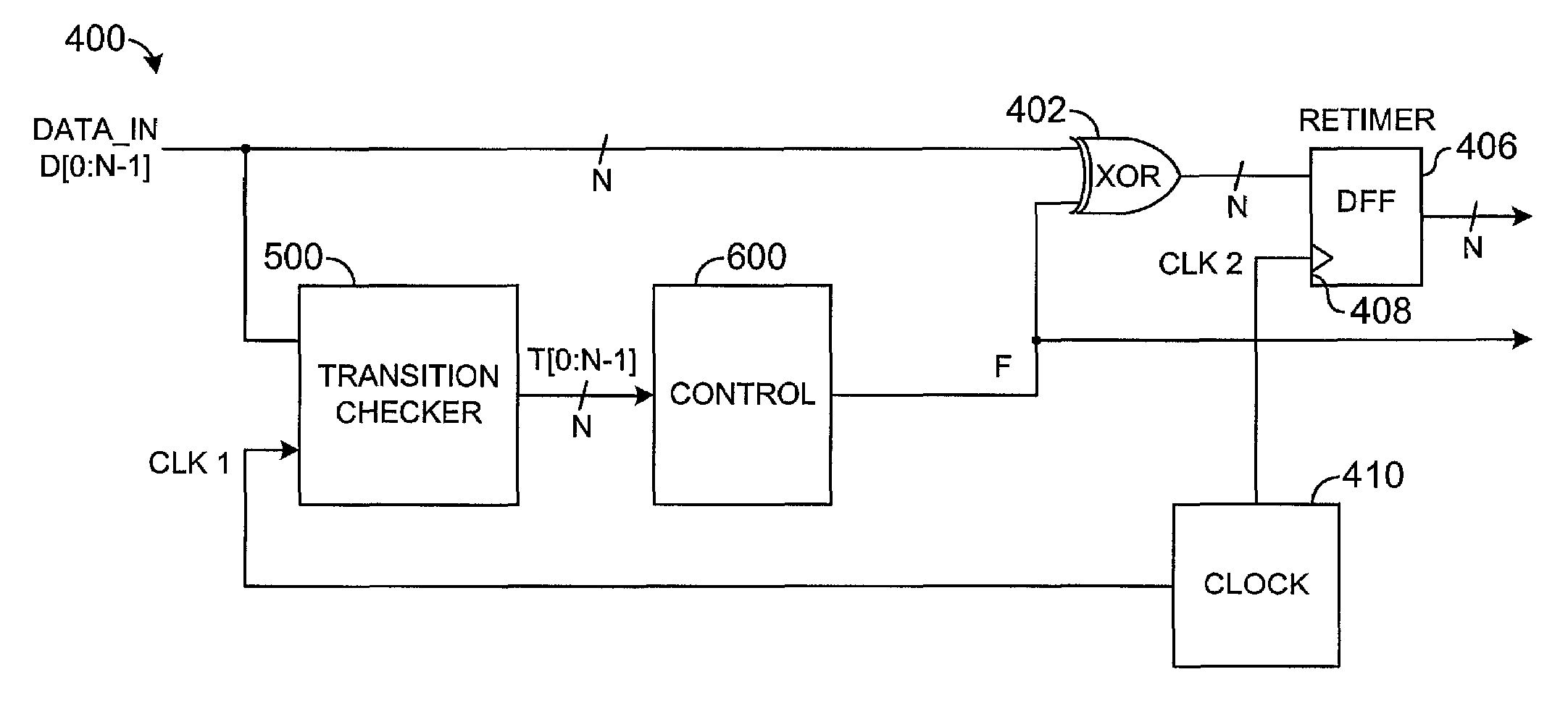
[0030]In general, ground bounce is more likely to cause a violation of a simultaneously switched output (SSO) number than power droop and thus the following description focuses on reducing the ground bounce in open drain buffers. The same principles may be applied to reducing the power droop in open source buffers. Likewise, the present invention may also be applied to buffers that actively pull high and actively pull low.

[0031]Referring now to FIG. 3, an example system is shown in accordance with a preferred embodiment of the present invention. The system generally includes an apparatus 300 and an apparatus 312 connected by a transmission bus. The apparatus 300 may be implemented as an integrated circuit (IC) having a core 302 with a number (e.g., N) of data lines 304, each numbered 0 to N−1, of a data bus connected to respective inputs of a group of I / O buffers 306 by way of an SSO doubler 400. The I / O buffers 306 may be powered from a single pair of VDD / VSS lines (not shown) conn...


PUM


Abstract

An integrated circuit comprises a microprocessor for generating data signals along a data bus by way of an inverter to a plurality of input / output switching buffers. The buffers pass the data signals to a transmission bus for onward transmission to a receiving integrated circuit. A respective drain and source supply power to the buffers. A transition checking circuit monitors the number of data signals on the data bus simultaneously switching from a first to a second logic state and a control circuit counts the number of the simultaneous switching data signals and generates a flag signal when the count exceeds half the number of buffers. The flag signal is applied to the inverter to invert all of the data signals on the bus.

Description

[0001]This application claims the benefit of United Kingdom Application No. 0024226.3 filed Oct. 4, 2000.FIELD OF THE INVENTION[0002]The present invention relates to a method and / or architecture for integrated circuit input / output switching generally and, more particularly, to the reduction of the impact of simultaneous switching noise in digital integrated circuits.BACKGROUND OF THE INVENTION[0003]In a digital integrated circuit (IC), a microprocessor core of the circuit is connected to external pins of the IC through input / output (I / O) switching buffers which pass data from the core of the IC to external pins for transmission via external transmission lines to a receiving IC. The I / O switching buffers need a considerable amount of current in order to drive the high external loads. Power for the I / O switching buffers is provided by way of one or more pairs of supply lines comprising a drain (power) VDD and a source (ground) VSS which are in turn connected to respective external pin...

Claims


Application Information

Patent Timeline
Patent Type & Authority Patents(United States)
IPC IPC(8): G06F11/00H03K19/003
CPCH03K19/00346
Inventor ALANI, ALAA F.HUNT, KENNETH S.
Owner AVAGO TECH WIRELESS IP SINGAPORE PTE
Why Eureka
Try Eureka