Scanner system

a scanning system and scanning beam technology, applied in the field of scanning surfaces, can solve the problems of uniform power of the long-distance beam of the oblong beam, and achieve the effects of reducing laser power, increasing overlap, and reducing laser power

Inactive Publication Date: 2006-05-16
LASER IMAGING SYST
View PDF28 Cites 46 Cited by
  • Summary
  • Abstract
  • Description
  • Claims
  • Application Information

AI Technical Summary

Benefits of technology

[0018]In an aspect of some preferred embodiments of the invention, an optimum scanning speed is provided for different sensitivities of photoresist. In general, a scanner may be used for a number of different types of photoresist of varying sensitivity. In principle, the scanning speed could be matched to the sensitivity by varying the scanning speed inversely with the speed of the photoresist. However, most large scanners utilize a large polygon scanner, which operates best over a relatively restricted range of speeds. Thus, in the prior art, in addition to possibly changing the scanning speed, it was necessary to reduce the laser power when scanning a high-speed photoresist. In this way, much of the sensitivity advantage of the photoresist would be lost.
[0019]In a preferred embodiment of the invention, in addition to the variation in speed of the scan as in prior art devices, the amount of overlap of successive swaths is varied, depending on the power requirements of the photoresist. Thus, for slow photoresist, the overlap is increased (by reducing the speed of movement of the printed circuit board). For faster photoresist, not only is the scan speed increased somewhat, but the amount of overlap is decreased. Thus, over a relatively wide range of powers the laser power is kept at a high, preferably a constant, optimized, level. This results in an optimum scanning speed and optimum power utilization for a wide variety of photoresist speeds.
[0020]An aspect of some preferred embodiments of the invention relates to improved determination of the position of the beam as it scans.
[0021]In a preferred embodiment of the invention, the testing beam is at the same wavelength as at least one spectral line of the writing beam. Furthermore, the testing beam is preferably derived from the same laser source that produces the writing beam, preferably by providing a splitter near the output of the source. In a preferred embodiment of the invention, the two beams travel parallel or nearly parallel paths for most of their length. In particular, the testing beam travels through all of the scanning optics (starting at least from the polygon) including, preferably, the f-θ lens. However, in a preferred embodiment of the invention, the two beams are not parallel. Rather they both lie in a plane that is perpendicular to the scan direction. Although the beams are neither boresighted nor parallel, they both travel through the same scanning optics and are nearly identically deflected. Thus, measurements made on the position of the test beam accurately reflect the position of the writing beam.

Problems solved by technology

Preferably, the oblong beam does not have uniform power in its long direction.

Method used


Image

  • Scanner system
  • Scanner system
  • Scanner system

Examples


Embodiment Construction

System Overview

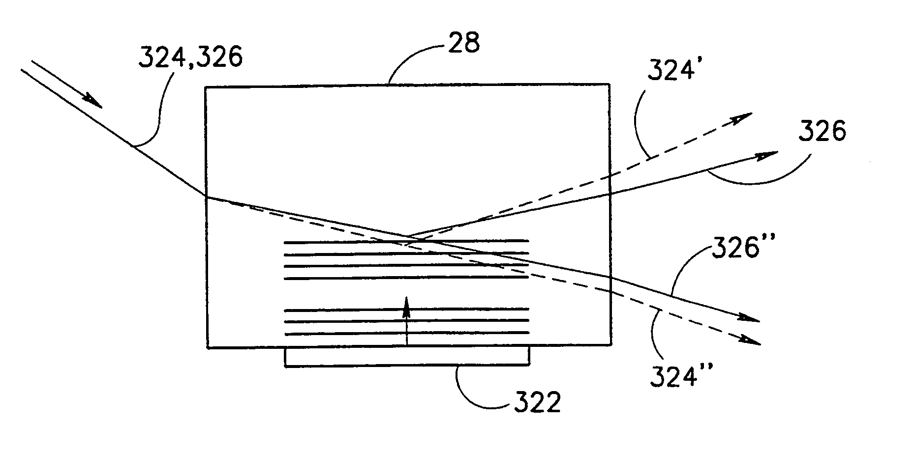
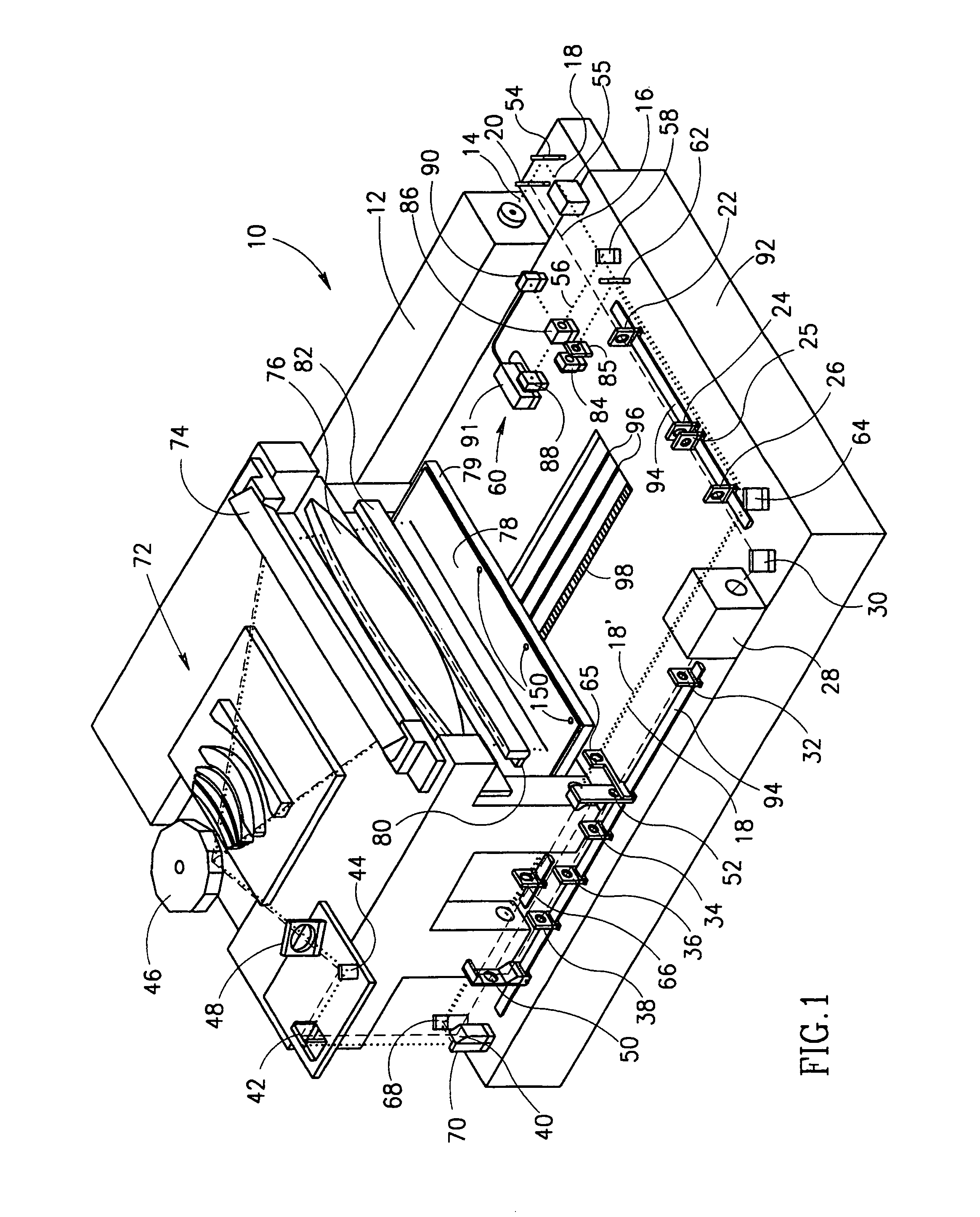
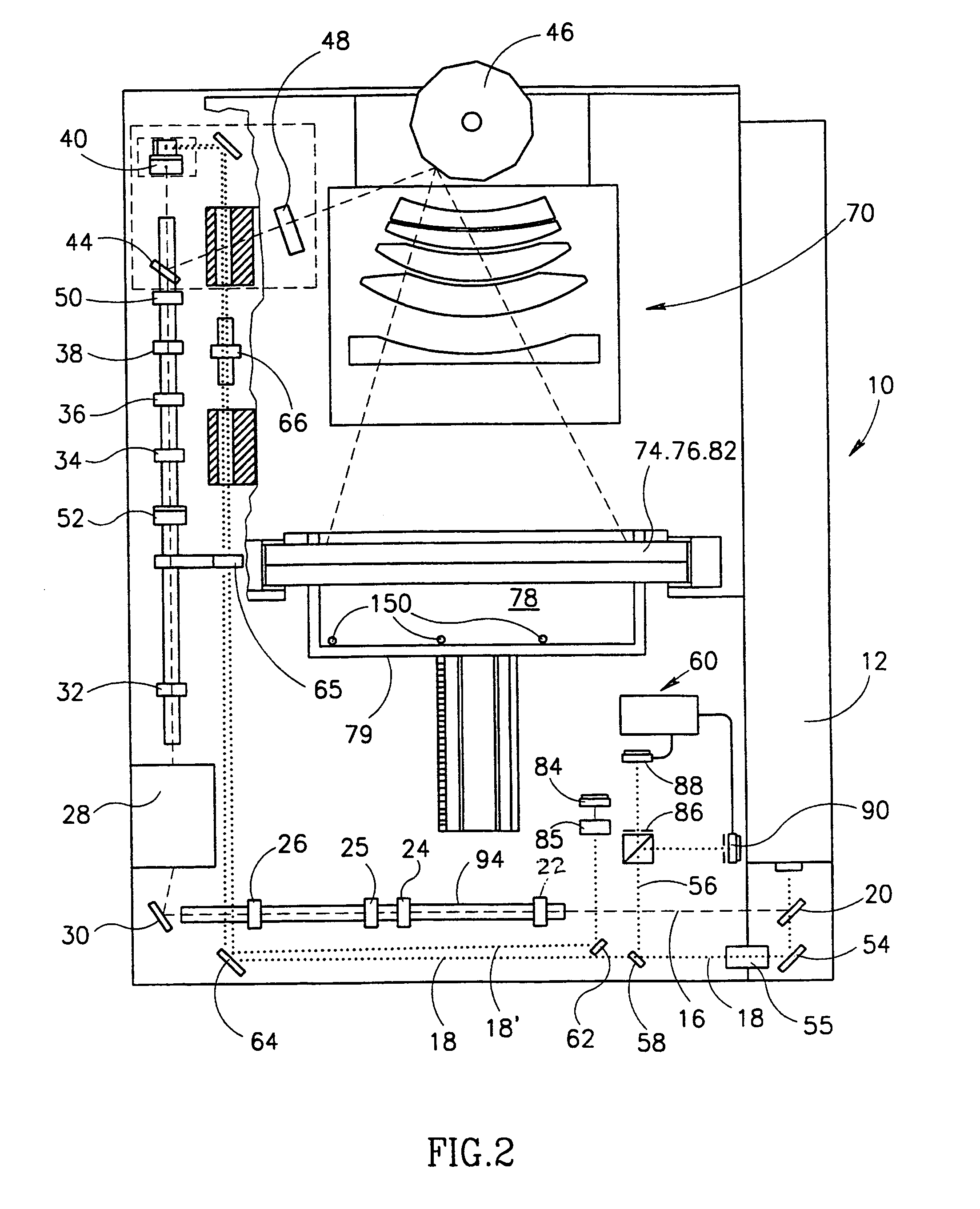
[0185]Reference is made to FIGS. 1–3, which show an exemplary direct writing printed circuit board scanner 10, in accordance with a preferred embodiment of the invention. Scanner 10 comprises a laser source 12, whose output wavelength is suitable for exposing a photoresist coating. In a preferred embodiment of the invention, an Argon Ion type ultraviolet laser, operating at 351.1 and 363.8 nanometers and delivering a maximum power of 4.4 watts has been found suitable. Such lasers are generally available and an Innova Sabre type laser of Coherent, Inc. of California USA or a Beam Lock 2085 type laser of Spectra Physics of California, USA, have both been found suitable. A beam 14 exits source 12 and is split into two beams, a main beam 16 and a test beam 18, by a first beam splitter (or partially reflective mirror) 20. As explained below, main beam 16 (shown as a dashed line), is (eventually) used to scan and expose the photoresist on the printed circuit board. Test bea...


PUM

PropertyMeasurementUnit
feature sizeaaaaaaaaaa

Abstract

A method of scanning for writing a pattern on a surface, including providing a scanning beam comprised of a plurality of independently addressable sub-beams, scanning the surface with the scanning beam a plurality of times, the sub-beams scanning the surface side-by-side in the cross-scan direction, each sub-beam being modulated to reflect information to be written, and overlapping the beams in successive scans in the cross scan direction such that all written areas of the surface are written on during at least two scans.

Description

RELATED APPLICATION[0001]This application is the US national stage of PCT Application PCT / EP99 / 01764, filed 15 Mar. 1999.FIELD OF THE INVENTION[0002]The present invention is related to methods for scanning surfaces, for example for writing on the surfaces with a scanning laser beam. In particular, a system for direct writing of patterns on printed circuit boards is disclosed.BACKGROUND OF THE INVENTION[0003]Most printed circuit boards are produced by first coating a printed circuit board substrate, having a solid copper cladding, with a photoresist material. When selectively exposed and developed, part of the photoresist is removed and the remaining photoresist forms a pattern corresponding to the light and dark areas of the illumination. After formation of the developed photoresist pattern, the copper cladding is typically subjected to an etching step in which that part of the copper cladding that is not coated by the photoresist is removed.[0004]In the main, one of two methods of ...

Claims


Application Information

Patent Timeline
Patent Type & Authority Patents(United States)
IPC IPC(8): B41J2/47B41J2/44G02B26/10G03F7/20G03F9/00G03G15/04G03G15/043H04N1/10H04N1/113H04N1/192H05K3/00H05K3/12
CPCG03F7/203G03F7/2051G03F7/2053G03F7/704G03F7/70775G03F9/00H04N1/192H05K3/0082H04N1/1135H04N2201/0471H04N2201/04718H04N2201/04732H04N2201/04737H04N1/1008
Inventor RETSCHKE, WOLFGANGSENF, WOLFGANGRUCKER, STEFFENKLOWSKY, UWEBATTIG, UDOBAUMANN, ULRICH
Owner LASER IMAGING SYST
Why Eureka
Try Eureka