Shift register with a built in level shifter

a technology of shift register and shift register, which is applied in the direction of logic circuit coupling/interface arrangement, digital storage, instruments, etc., can solve the problems of high manufacturing cost, low reliability, and high manufacturing cost of lcd, and achieve the effect of lowering the minimum voltage level of an input signal

Active Publication Date: 2006-05-23
LG DISPLAY CO LTD
View PDF16 Cites 48 Cited by
  • Summary
  • Abstract
  • Description
  • Claims
  • Application Information

AI Technical Summary

Benefits of technology

[0021]An advantage of the present invention is to provide a shift register that employs only a thin film transistor of the same type channel and has a built-in level shifter, which can lower the minimal voltage level of an input signal.
[0022]Another advantage of the present invention is to provide a scanning driver including a shift register with a built-in level shifter.
[0023]Still another advantage of the present invention is to provide a data driver including a shift register with a built-in level shifter.
[0024]Still another advantage of the present invention is to provide a liquid crystal display including a shift register with a built-in level shifter.
[0025]In order to achieve these and other advantages of the invention, a shift register with a built in level shifter according to the present invention includes a plurality of stages connected in cascade for shifting a start pulse inputted through an input terminal and sequentially outputting the shifted pulse; and a plurality of level shifters for level-shifting a voltage level of the shifted pulse applied from each of the stages and outputting it.
[0026]A scanning driver for applying a scanning pulse to scanning lines of a display panel according to the present invention has a shift register that includes a plurality of stages connected in cascade for shifting a start pulse inputted through an input terminal and sequentially outputting the shifted pulse; and a plurality of level shifters for level-shifting a voltage level of the shifted pulse applied from each of the stages and outputting it as the scanning pulse.

Problems solved by technology

Further, use of the amorphous silicon type thin film transistor is disadvantageous in that it results in higher manufacturing costs of the LCD as peripheral driving circuits, such as the gate driver and the data driver, need to be manufactured separately and mounted in the liquid crystal display panel.
Because there are included both P and N channels in case of using the CMOS thin film transistors, it is advantageous that the driving voltage has a wide range and it is easier to make an integrated circuit, however, there is a disadvantage that the manufacturing cost is high and the reliability is low since a number of processes are required.
In other words, it is difficult to ensure device characteristics while generating a voltage having a swing width more than 10V or a negative voltage and, hence, to manufacture an IC on a single chip.
This configuration is disadvantageous that an external circuit mounted on the PCB 20 is made to be compact with great difficulty.
Furthermore, since a clock signal including positive and negative voltages and having a swing width of 10V or more must be applied from the external circuit to the data shift register 14 and the gate shift register 16 of the liquid crystal display panel 10, a problem of a large power consumption is encountered.

Method used


Image

  • Shift register with a built in level shifter
  • Shift register with a built in level shifter
  • Shift register with a built in level shifter

Examples


Embodiment Construction

[0066]Reference will now be made in detail to embodiments of the present invention, examples of which are illustrated in the accompanying drawings.

[0067]Referring to FIG. 4, there is shown a block diagram of a shift register with a built in level shifter according to an embodiment of the present invention.

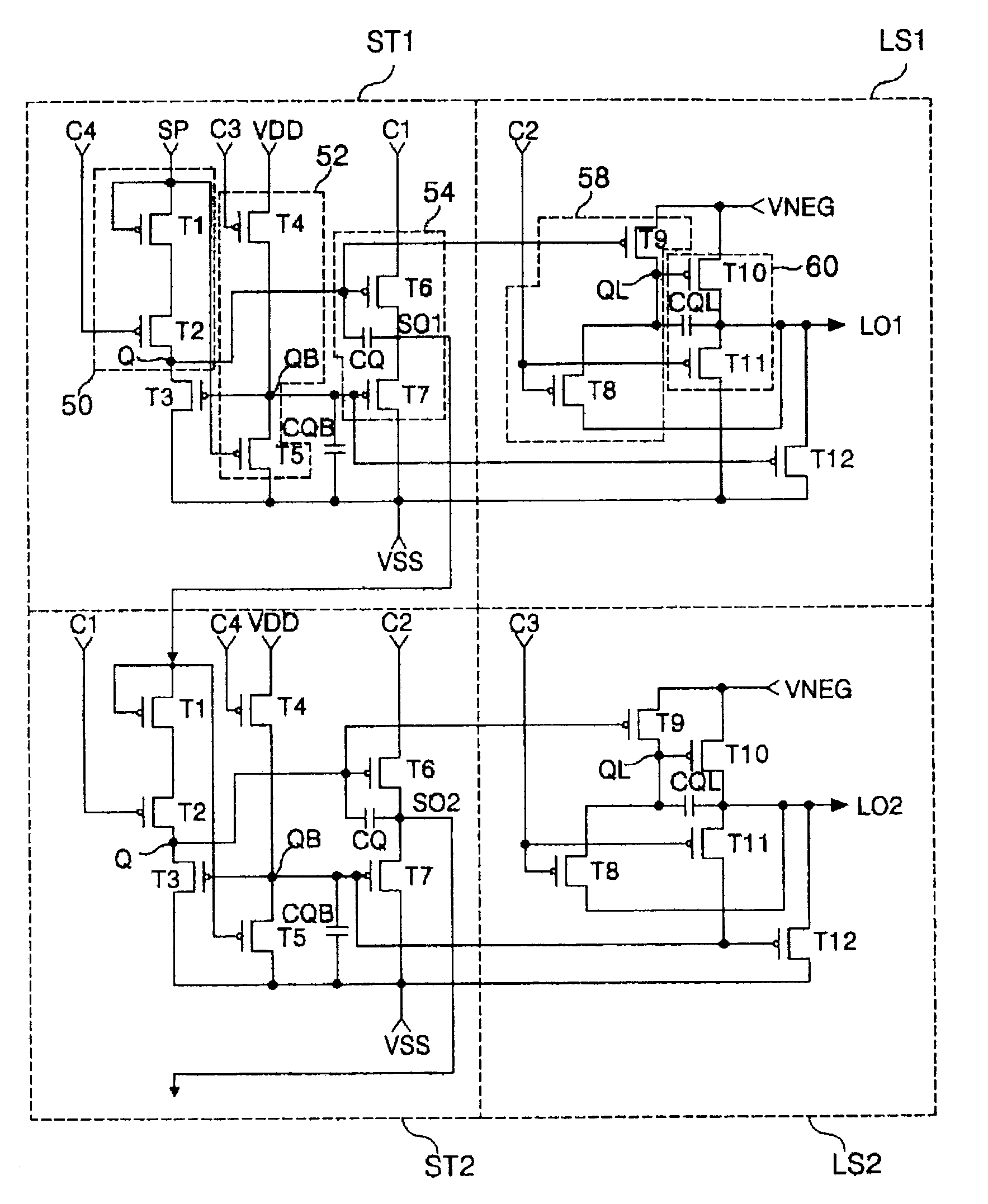
[0068]The shift register with the built in level shifter includes a shift stage array 32 consisting of n shift stages ST1 to STn connected to an input line of a start pulse SP in cascade and a level shifter array 34 consisting of level shifters LS1 to LSn connected to each output terminal of the stages ST1 to STn.

[0069]In the shift register array 32, the start pulse SP is inputted to the first stage ST1, and output signals of each of the previous stages are inputted to the second to nth stages ST2 to STn, respectively. The stages ST1 to STn receive three clock signals of the first to fourth clock signals C1 to C4 via first, second, and third clock signal input lines. Each of the fi...


PUM

PropertyMeasurementUnit
swing voltageaaaaaaaaaa
voltageaaaaaaaaaa
voltageaaaaaaaaaa

Abstract

A shift register employs only a thin film transistor of the same type channel and has a level shifter built-in. A shift register with a built in level shifter includes a plurality of stages and a plurality of level shifters. The stages are connected in cascade to shift a start pulse inputted through an input terminal and sequentially output the shifted pulse. The level shifters level-shift a voltage level of the shifted pulse applied from each of the stages and outputting it.

Description

[0001]This application claims the benefit of Korean Patent Application No. P2001-78450, filed on Dec. 12, 2001 and P2002-65541, filed on Oct. 25, 2002, which is hereby incorporated by reference for all purposes as if fully set forth herein.BACKGROUND OF THE INVENTION[0002]1. Field of the Invention[0003]The present invention relates to a shift register circuit, and more particularly to a shift register that employs only a thin film transistor of the same type channel and has a level shifter built-in. And, the present invention relates to a scanning driver, a data driver and a liquid crystal display having the shift register.[0004]2. Description of the Related Art[0005]Generally, a liquid crystal display LCD displays a picture using an electric field to control the light transmittance of a liquid crystal. To this end, the LCD includes a liquid crystal display panel having liquid crystal cells arranged in a matrix, and a driving circuit which drives the liquid crystal display panel. Wi...

Claims


Application Information

Patent Timeline
Patent Type & Authority Patents(United States)
IPC IPC(8): G09G3/36G02F1/133G09G3/20G11C19/00G11C19/18G11C19/28H03K19/0185
CPCG09G3/3677G09G3/3688G11C19/282G11C19/00G11C19/184G09G2310/0289
Inventor KIM, BYEONG KOOPARK, JAE DEOKHA, YONG MIN
Owner LG DISPLAY CO LTD
Why Eureka
Try Eureka