Heat sink structure with embedded electronic components for semiconductor package

a technology of electronic components and semiconductor packages, which is applied in the direction of semiconductor/solid-state device details, cooling/ventilation/heating modifications, semiconductor devices, etc., can solve the problems of significant increase in manufacturing and material costs, large amount of heat, and damage to the performance and lifetime so as to improve the electric performance of the semiconductor package, eliminate electromagnetic interference, and improve heat dissipation

Active Publication Date: 2006-05-23
PHOENIX PRECISION TECH CORP
View PDF9 Cites 56 Cited by
  • Summary
  • Abstract
  • Description
  • Claims
  • Application Information

AI Technical Summary

Benefits of technology

[0008]In accordance with the foregoing drawbacks of the prior art, a primary objective of the present invention is to provide a heat sink structure with embedded electronic components for a semiconductor package, which can improve heat dissipation, eliminate electromagnetic interference and enhance electric performance of a semiconductor package with the heat sink structure.
[0009]Another objective of the invention is to provide a heat sink structure with embedded electronic components for a semiconductor package so as to enhance the flexibility of routability or circuit layout on a substrate of a semiconductor package with the heat sink structure.
[0010]A further objective of the invention is to provide a heat sink structure with embedded electronic components for a semiconductor package so as not to complicate the manufacturing processes and to increase the fabrication cost.
[0011]In order to achieve foregoing and other objectives, the present invention proposes a heat sink structure with embedded electronic components comprising a heat sink formed with a plurality of recessed cavities for embedding the electronic components and receiving at least one semiconductor chip therein. The heat sink with at least one embedded electronic component can be attached to a substrate mounted with at least one semiconductor chip to form a semiconductor package, wherein the at least one semiconductor chip is received in at least one of the recessed cavities. Besides improving the heat dissipating efficiency, the heat sink with the electronic component can enhance electric performance of the semiconductor package and provides a shielding effect to protect the semiconductor chip against external electromagnetic interference.
[0012]The electronic component embedded in the heat sink can be an active or passive component. The passive component may be for example a capacitor, resistor, inductor or chip-type passive component. Moreover, since the active / passive component is embedded and the semiconductor chip of the semiconductor package is received in the recessed cavities of the heat sink, this arrangement does not need to require the complex manufacturing processes for integrating a passive component in the conventional semiconductor package substrate and would not increase the fabrication cost unlike the case of the prior art to re-design the conventional substrate to achieve desirable electric performance. As a result, in the use of the heat sink structure according to the present invention, routability or circuit layout on the substrate can be improved.

Problems solved by technology

However, such an integral substrate has complex structure to be fabricated and thus is cost-ineffective in manufacture; moreover, the substrate needs to be re-designed if different property values such as resistance value and capacitance value are required, which would significantly increase the manufacturing and material costs.
In addition, electronic components and electronic circuits are packed in high density in the semiconductor package and thus produce a huge amount of heat.
If the heat cannot be timely dissipated in an efficient way, the performance and lifetime of the semiconductor package would be damaged by overheat.
Furthermore, the semiconductor package generally lacks a shielding mechanism and is easily interfered by external electromagnetic waves and noises.

Method used


Image

  • Heat sink structure with embedded electronic components for semiconductor package
  • Heat sink structure with embedded electronic components for semiconductor package
  • Heat sink structure with embedded electronic components for semiconductor package

Examples


first embodiment

[0025]FIG. 3 shows a semiconductor package in the use of the heat sink structure with embedded electronic components according to the

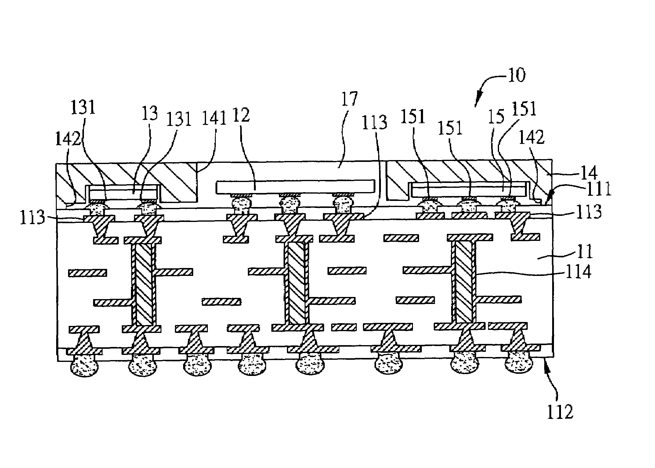
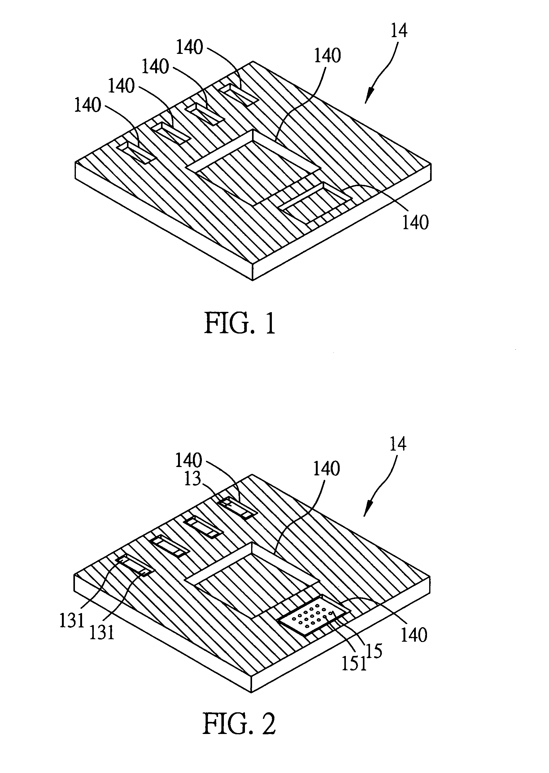
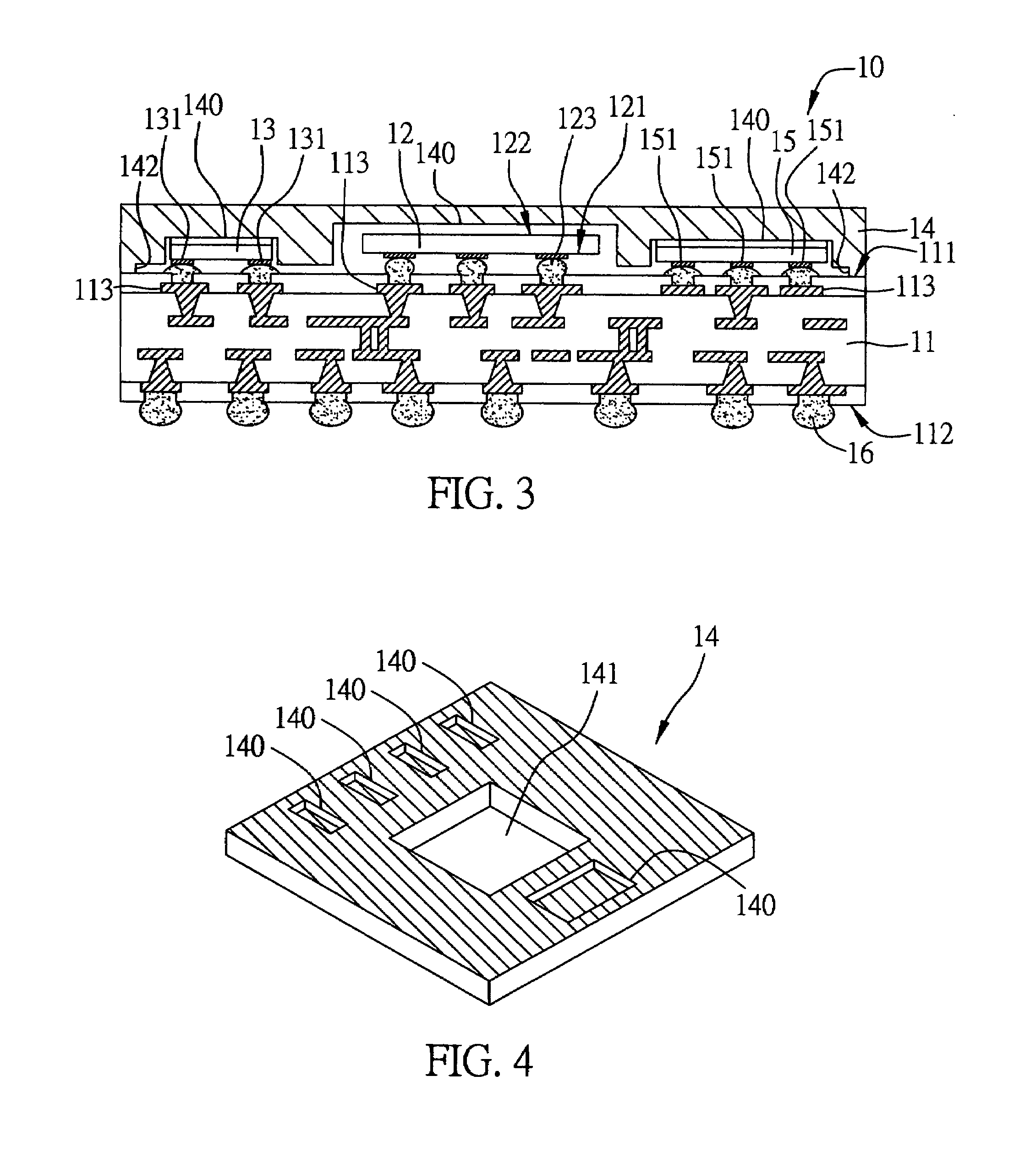
[0026]As shown in FIG. 3, the semiconductor package 10 comprises a substrate 11 having a first surface 111 and a second surface 112, with at least one semiconductor chip 12 mounted in a flip-chip package technique on the first surface 111 and electrically connected to electrical connection pads 113 on the first surface 111 of the substrate 11; and the beat sink 14 having the recessed cavities 140 formed on the lower surface thereof, wherein the recessed cavities 140 includes those embedded with the passive components 13, 15 and at least one corresponding in position to the chip 12. When the lower surface of the heat sink 14 is attached to the first surface 111 of the substrate 11, the passive components 13, 15 embedded in the recessed cavities 140 of the heat sink 14 are electrically connected via their electrodes 131, 151 to the electrical connection ...

second embodiment

[0033]FIG. 6 shows a semiconductor package in the use of the heat sink structure with embedded electronic components according to the

[0034]As shown in FIG. 6, the semiconductor package 10 of the second embodiment is substantially the same as that of the first embodiment, but only differs in that in this embodiment the at least one semiconductor chip 12 mounted on the first surface 111 of the substrate 11 is received in the at least one through hole 141 of the heat sink 14. A molding process is performed to fill a resin compound such as epoxy resin in the through hole 141 and the space between the heat sink 14 and the substrate 11 to form an encapsulation body 17 that encapsulates and protects the chip 12 against damage from external moisture or contaminant. The encapsulation body 17 also helps alleviate the thermal stresses generated by CTE mismatch between the heat sink 14 and the substrate 11. Moreover, the substrate 11 is formed with a plurality of plated through holes (PTHs) 114...


PUM


Abstract

A heat sink structure with embedded electronic components is proposed, wherein a plurality of recessed cavities are formed on a heat sink for embedding the electronic components and receiving at least one semiconductor chip therein. This arrangement enhances electric performance of a semiconductor package with the above heat sink structure and improves heat dissipating efficiency of the semiconductor package.

Description

FIELD OF THE INVENTION[0001]The present invention relates to heat sink structures with embedded electronic components for semiconductor packages, and more particularly, to an integrated structure of a heat sink and electronic components, which can significantly improve electric performance and heat dissipation efficiency of a semiconductor package with such an integrated structure.BACKGROUND OF THE INVENTION[0002]BGA (Ball Grid Array) is an advanced type of integrated circuit packaging technology which is characterized in mounting at least one semiconductor chip on a front surface of a substrate and implanting an array of solder balls on a back surface of the substrate. The solder balls act as input / output (I / O) connections to electrically connect the chip to an external device such as printed circuit board (PCB). The BGA configuration advantageously allows relatively more solder balls or I / O connections to be accommodated on a unit area of the substrate in accordance with high inte...

Claims


Application Information

Patent Timeline
Patent Type & Authority Patents(United States)
IPC IPC(8): H05K7/20H01L23/367H01L25/065
CPCH01L23/367H01L25/0655H01L2924/09701H01L2924/15311H01L2924/16153H01L2924/19105H01L2924/3025H01L23/552H01L2224/16225H01L2224/32245H01L2224/73253H01L23/3128H01L23/3675H01L23/4334H01L23/49816H01L23/49827H01L2224/16227H01L2224/05573H01L2224/05568H01L2924/00014H01L2224/05599
Inventor HSU, SHIH-PINGWONG, LIN-YIN
Owner PHOENIX PRECISION TECH CORP
Why Eureka
Try Eureka