Cutting tool with sensor and production method therefor

a technology of cutting tool and sensor, which is applied in the direction of shaping cutters, metal-working equipment, turning machine accessories, etc., can solve the problems of inability to provide satisfactory sensitivity and reliability, difficult quantitative determination of in-process wear amount, and inability to directly observe the wear of the tool during the machining in the machining environment. , to achieve the effect of improving the insulation reliability of the insulation film

Inactive Publication Date: 2006-05-30
KYOCERA CORP
View PDF13 Cites 21 Cited by
  • Summary
  • Abstract
  • Description
  • Claims
  • Application Information

AI Technical Summary

Benefits of technology

[0018]This arrangement improves the insulation reliability of the insulation

Problems solved by technology

However, it is very difficult in view of a machining environment to directly observe the wear of the tool during the machining.
However, the quantitative determination of the wear amount on an in-process basis is difficult, failing to provide satisfactory sensitivity and reliability.
Where a cemented carbide substrate or a cermet substrate is coated with the aluminum oxide film which has a thermal expansion coefficient different from that of the substrate by the CVD method, the aluminum oxide film suffers from minute cracks extending to the substrate after the coating.
Where the aluminum oxide film is formed by the PVD method, the aluminum oxide film suffers from defects such as pinholes extending to the substrate, and the electrically conductive substrate and the electrically conductive sensor film are shorted through the pinholes.
These problems make it ve

Method used


Image

  • Cutting tool with sensor and production method therefor
  • Cutting tool with sensor and production method therefor
  • Cutting tool with sensor and production method therefor

Examples


example 1

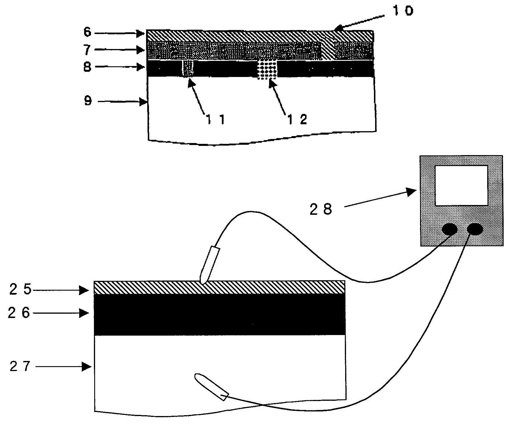
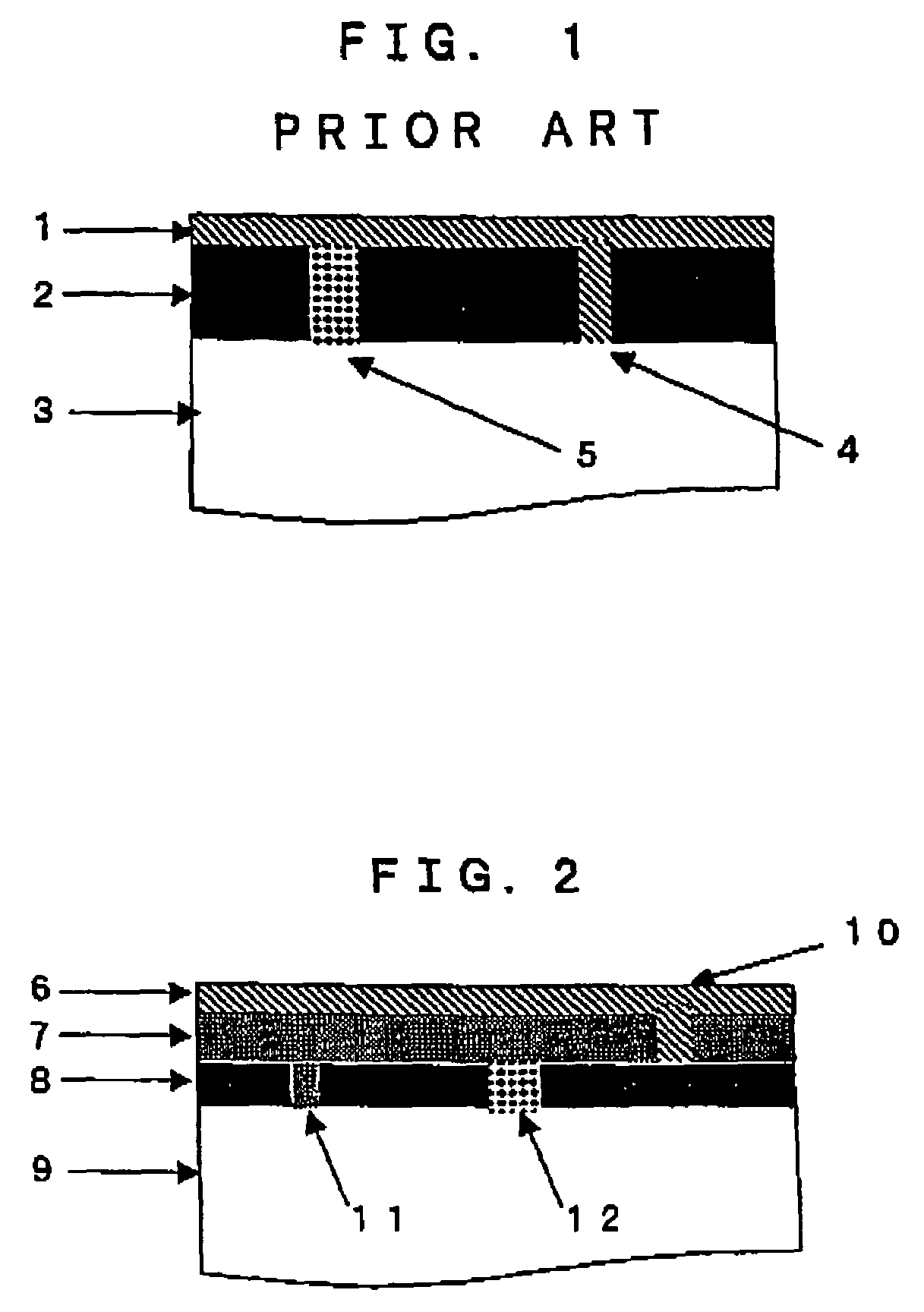
[0070]Five samples according to Example 1 (Samples 1) were each produced in the following manner. An Al2O3—TiC ceramic substrate was employed as an electrically conductive substrate. An aluminum oxide film having a thickness of 3 μm was formed on the substrate by sputtering for formation of a first insulation layer for insulating an electrically conductive film from the electrically conductive substrate. More specifically, a high-frequency sputtering apparatus employing an Al2O3 target was used for the sputtering. In an Ar atmosphere, 3-minute pre-sputtering, 12-minute etching on the substrate and 15-minute pre-sputtering for cleaning the target were carried out, followed by 60-minute main sputtering for the formation of the first insulation layer.

[0071]Subsequently, another aluminum oxide film having a thickness of 3 μm was formed on the first insulation layer by sputtering for formation of a second insulation layer. More specifically, a high-frequency sputtering apparatus employin...

example 2

[0074]Five samples according to Example 2 (Samples 3) were each produced in the following manner. An Al2O3—TiC ceramic substrate was employed as an electrically conductive substrate. An aluminum oxide film having a thickness of 3 μm was formed on the substrate by sputtering for formation of a first insulation layer for insulating an electrically conductive film from the electrically conductive substrate. More specifically, a high-frequency sputtering apparatus employing an Al2O3 target was used for the sputtering. In an Ar atmosphere, 3-minute pre-sputtering, 12-minute etching on the substrate and 15-minute pre-sputtering for cleaning the target were carried out, followed by 60-minute main sputtering for the formation of the first insulation layer. Subsequently, another aluminum oxide film having a thickness of 5 μm was formed on the first insulation layer by sputtering for formation of a second insulation layer. More specifically, a high-frequency sputtering apparatus employing an ...

example 3

[0077]A sample according to Example 3 was produced in the following manner. An Al2O3—TiC ceramic substrate was employed as an electrically conductive substrate. An aluminum oxide film having a thickness of 1 μm was formed on the substrate by sputtering for formation of a first insulation layer for insulating an electrically conductive film from the electrically conductive substrate. More specifically, a high-frequency sputtering apparatus employing an Al2O3 target was used for the sputtering. In an Ar atmosphere, 3-minute pre-sputtering, 12-minute etching on the substrate and 15-minute pre-sputtering for cleaning the target were carried out, followed by 20-minute main sputtering for the formation of the first insulation layer. Subsequently, another aluminum oxide film having a thickness of 5 μm was formed on the first insulation layer by sputtering for formation of a second insulation layer. More specifically, a high-frequency sputtering apparatus employing an Al2O3 target was used ...


PUM

PropertyMeasurementUnit
Lengthaaaaaaaaaa
Lengthaaaaaaaaaa
Electrical resistanceaaaaaaaaaa

Abstract

A cutting tool with a sensor according to the present invention includes an electrically conductive substrate, an insulation film provided on a surface of the electrically conductive substrate, and a sensor circuit of an electrically conductive film provided on the insulation film. The insulation film includes two consecutive insulation layers. Even if the plural insulation layers each have defects such as cracks and pinholes which possibly impair the insulation property impair the insulation film, the defects present in the plural layers are unlikely to be continuous. Therefore, the insulation film has an improved insulation reliability, thereby ensuring proper function of the sensor circuit in the cutting tool.

Description

BACKGROUND OF THE INVENTION[0001]1. Field of the Invention[0002]The present invention relates to a cutting tool and a production method therefor. More particularly, the invention relates to a cutting tool having a sensor circuit for detecting the end of the service life of the cutting tool and to a production method therefor.[0003]2. Description of Related Art[0004]The end of the service life of a cutting tool having a cutting edge defined along an intersection ridge between a rake face and a flank is generally judged on the basis of the amount of wear of the flank. For highly accurate machining, it is imperative to speedily determine the amount of the wear of the flank on an in-process basis during a cutting operation. However, it is very difficult in view of a machining environment to directly observe the wear of the tool during the machining.[0005]Therefore, the determination of the amount of the wear of the tool is generally achieved by interrupting the machining, detaching the ...

Claims


Application Information

Patent Timeline
IPC IPC(8): B23B27/16B23B27/14B23Q17/09C04B35/10C04B35/584C04B41/52C04B41/89
CPCB23B27/145B32B18/00C04B35/10C04B35/5611C04B35/5626C04B35/58014C04B35/58021C04B35/584C04B41/009C04B41/52C04B41/89B23Q17/09C04B41/4529C04B41/5031C04B41/524C04B41/5068C04B35/117Y10T409/30728C04B2235/3217C04B2235/3224C04B2235/3272C04B2235/3275C04B2235/34C04B2235/3418C04B2235/3839C04B2235/3843C04B2235/3856C04B2235/3873C04B2235/3886C04B2235/405C04B2235/80Y10T407/23Y10T407/28Y10T407/27B23Q17/0952
Inventor FUKANO, TSUYOSHI
Owner KYOCERA CORP
Why Eureka
Try Eureka