Process for thick film circuit patterning
a technology of circuit patterning and thick film, which is applied in the direction of resistor manufacturing, metal pattern materials, liquid/solution decomposition chemical coating, etc., can solve the problems of thin film etch patterning approach for display and other applications, thin film photo-patterning method, and narrow particle size distribution window
- Summary
- Abstract
- Description
- Claims
- Application Information
AI Technical Summary
Benefits of technology
Problems solved by technology
Method used
Image
Examples
example 1
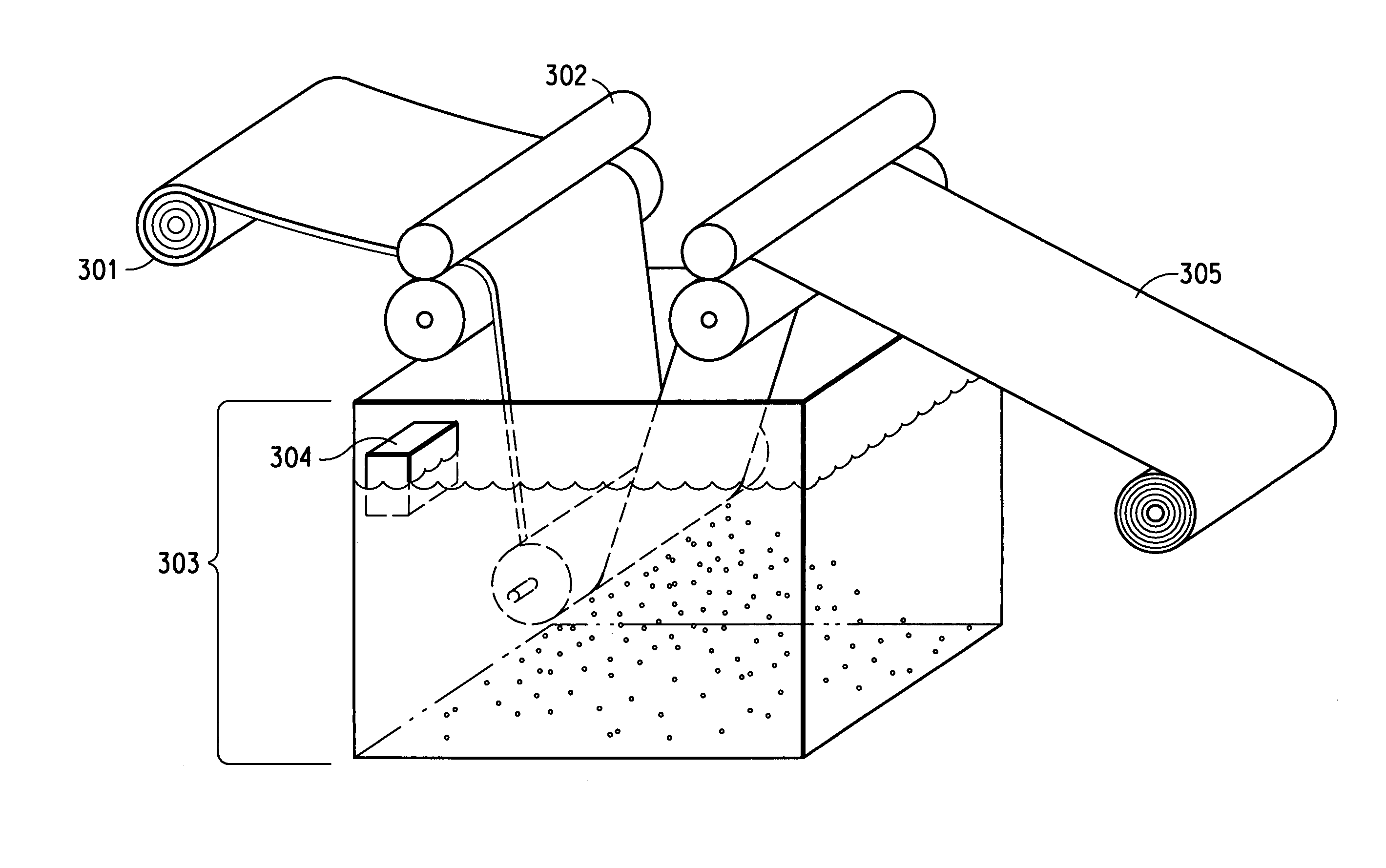
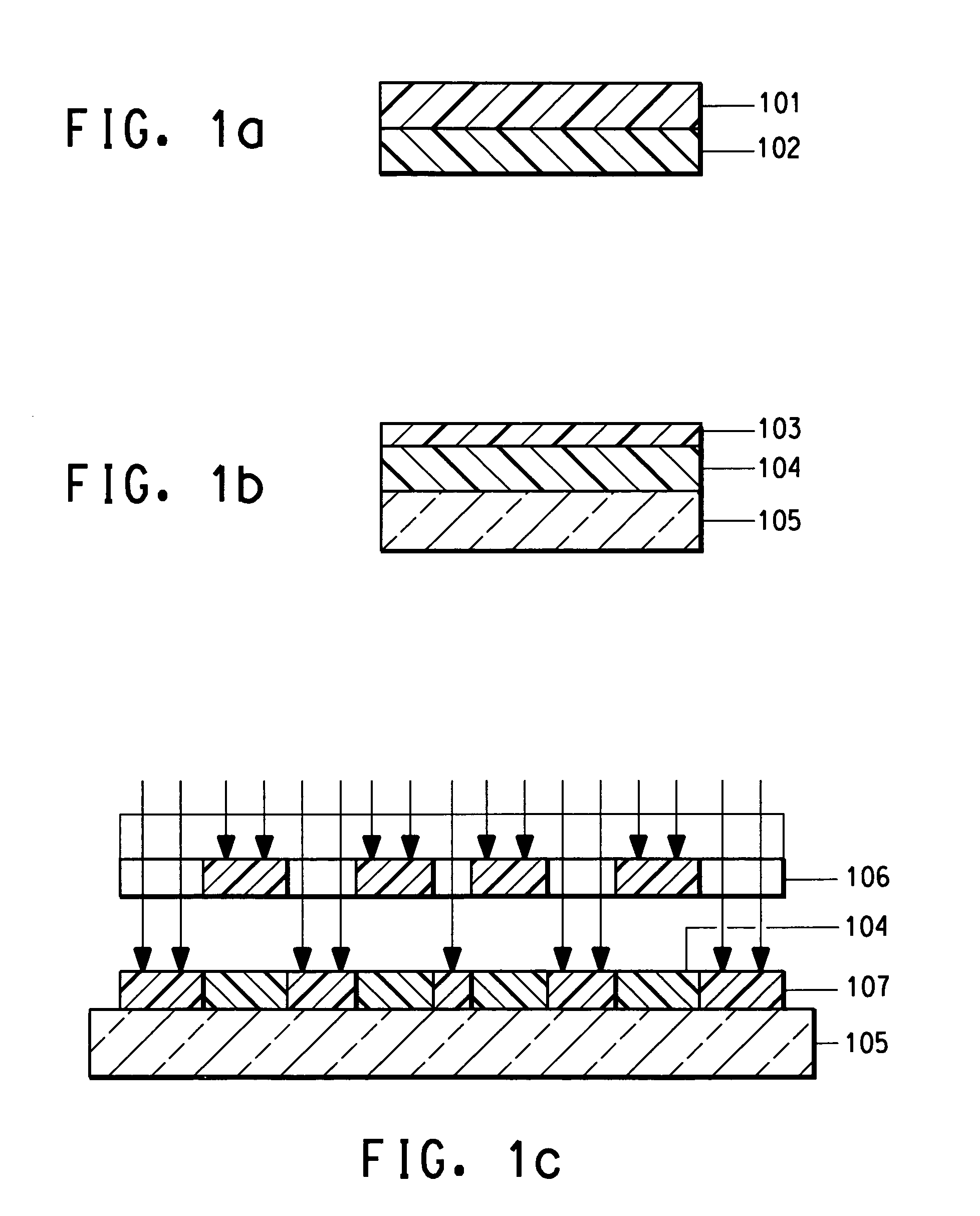
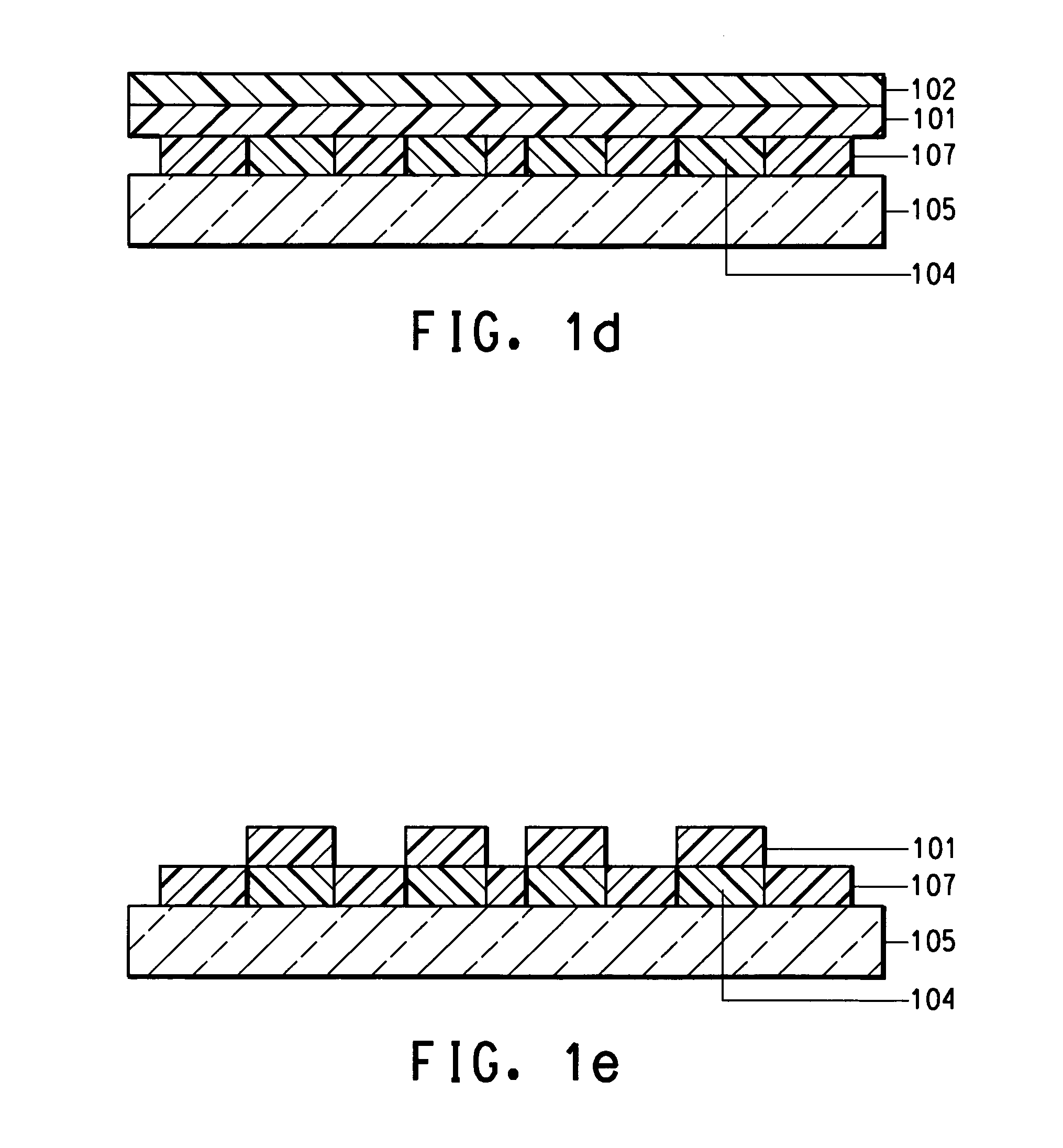
[0072]A positive CROMALIN® film, type ICFD (made by E. I. du Pont de Nemours and Company, Wilmington, Del.), having a coating weight in the range of 300 mg / dm2, was laminated (after peeling the removable base layer) to a soda lime glass substrate at about 250 d / F. The CROMALIN® film was exposed using a photomask circuit pattern (5KW UV bulb) for 15 units. The cover sheet on the imaged CROMALIN® film was peeled off. A transfer sheet was laminated onto the imaged film (with the thick film side of the transfer sheet facing the imaged layer). Peeling the transfer sheet produced the desired pattern where the unexposed areas of the imaged film layer remained tacky and the thick film was disposed on the tacky areas. The structure was fired at 500° C. in air using a standard thick film firing profile for displays. The imaged film was completely burned out and the sintered, patterned thick film adhered strongly to the soda lime glass substrate. There was no detectable adhesion difference bet...
example 2
[0073]The same process as Example 1 was repeated with the exception of no exposure of a CROMALIN® film and processed at a firing temperature of 585° C. The CROMALIN® film (completely covered by the thick film composition of the transfer sheet) was burned out and adhesion of the thick film composition across the substrate surface was obtained.
example 3
[0074]The same process as Example 2 was repeated 6 times (imaged film / thick film composition / imaged film / thick film composition, etc.) and the six-layer imaged film / thick film composition was cofired at 585° C. Similarly, all six layers of the imaged film were burned out and a thick film layer adhered to the glass substrate.
PUM
| Property | Measurement | Unit |
|---|---|---|
| smoothness | aaaaa | aaaaa |
| smoothness | aaaaa | aaaaa |
| temperature | aaaaa | aaaaa |
Abstract
Description
Claims
Application Information


