Layer-thickness detection methods and apparatus for wafers and the like, and polishing apparatus comprising same

a technology of thickness detection and wafers, applied in the direction of lapping machines, semiconductor/solid-state device testing/measurement, instruments, etc., can solve the problems of uneven surface, short focal range of projection optics used in such apparatuses, and inability to detect uniform surfaces, etc., to achieve simple and convenient detection

Inactive Publication Date: 2006-05-30
NIKON CORP
View PDF25 Cites 59 Cited by
  • Summary
  • Abstract
  • Description
  • Claims
  • Application Information

AI Technical Summary

Benefits of technology

[0018]In view of the above-summarize shortcomings of the prior art, an object of the invention is to provide, inter alia, simple and convenient detection methods by which the...

Problems solved by technology

Projection optics used in such apparatus have extremely short focal ranges.
The focal ranges are now so short that the uneven surface that results from stacking multiple layers atop one another during manufacture of an integrated circuit is no longer in sharp focus from peaks to valleys of the surface.
Whereas several candidate techniques have now been developed for performing planarization, as summarized below, a key problem has been how to accurately detect, during planarization, when to stop planarizing so as to ensure the desired amount of material has been removed without removing excessive material.
Unfortunately, achieving consistent results with CMP is much more difficult than with other semiconductor processing steps such as layer-forming and etching.
Unfortunately, monitoring polishing by monitoring torque is notoriously inaccurate and unreliable.
Unfortunately, the “blank”-measurement method has several serious disadvantages.
First, the method requires considerable time to execute and to provide feedback to the actual polishing process.
Because the size of the blank region is normally very small, the range of measurements that can be performed at the location is also very small.
Available apparatus for accurately measuring layer thickness within such a small area are simply not available.
It is also very difficult to perform measurements in such a small area at sufficiently high speed because the required mechanism for picking up, recognizing, and processing the image of the blank region is very complex.
Also, positioning the wafer for measurement at the blank location poses many problems.
Another substantial contributor to the excessive amount of time required to perform the “blank” technique is the need to interrupt polishing, clean the wafer, and transport the wafer to a remote but stable location for measure...

Method used


Image

  • Layer-thickness detection methods and apparatus for wafers and the like, and polishing apparatus comprising same
  • Layer-thickness detection methods and apparatus for wafers and the like, and polishing apparatus comprising same
  • Layer-thickness detection methods and apparatus for wafers and the like, and polishing apparatus comprising same

Examples


first embodiment

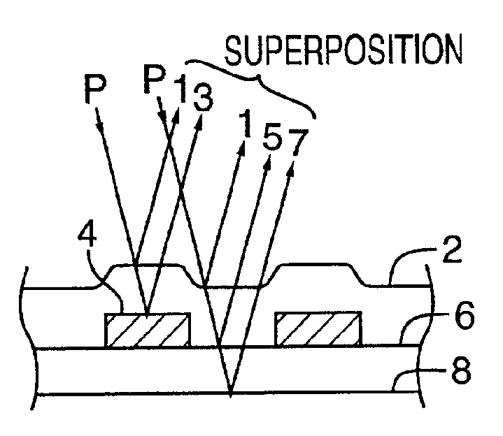
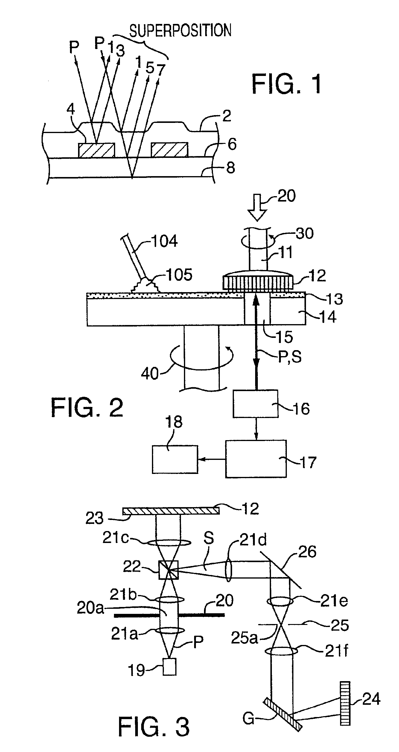
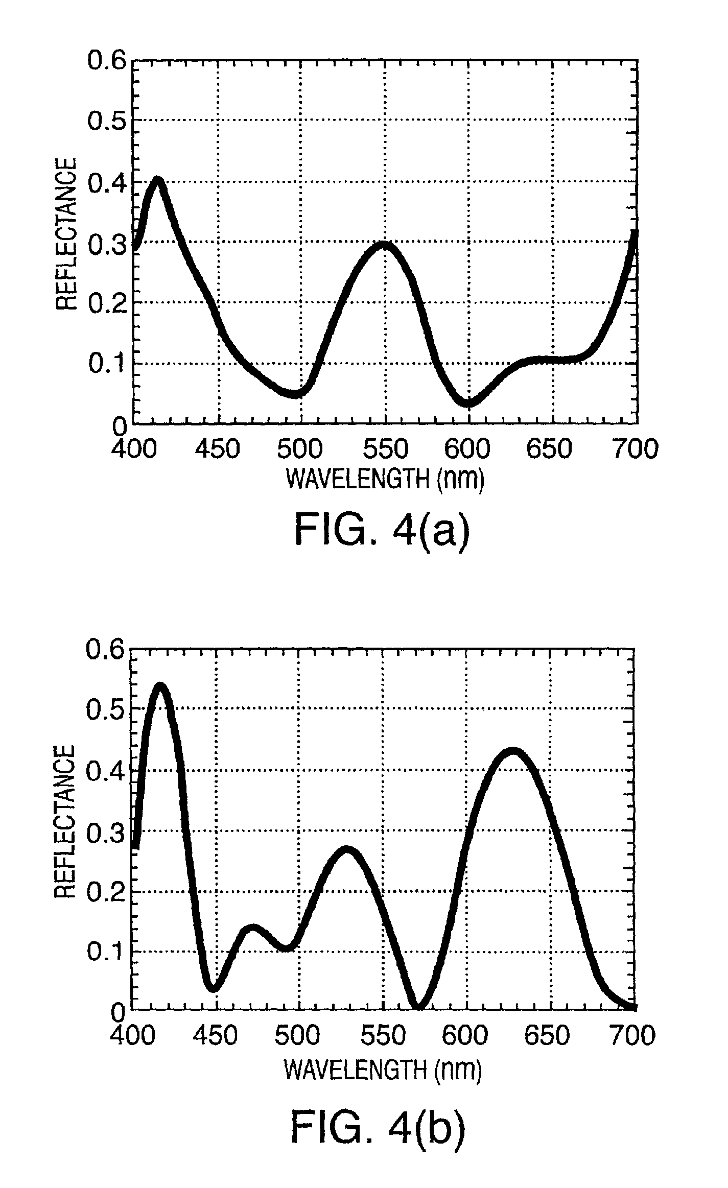
[0075]In this embodiment, wavelengths corresponding to local maxima of the spectral reflectance and wavelengths corresponding to local minima of the spectral reflectance are obtained by processing a spectral reflectance signal within the measurement wavelength range. Such local maxima and minima (along with their corresponding wavelengths) are used as measurement parameters of the spectral characteristic. For example, a polishing endpoint for a patterned wafer undergoing CMP can be detected with high accuracy by monitoring changes in the local maxima signals or changes in the local minima signals.

[0076]Besides simply local maxima and local minima of spectral reflectance, other useful parameters for measurement purposes are differences (e.g., local maximum−local minimum) and quotients (e.g., local maximum / local minimum). Also, in place of local maxima, the largest local maximum obtained in the measured wavelength range of the spectral reflectance can be used as a measurement paramete...

second embodiment

[0080]In the second embodiment, the wavelength dispersion of a reflectance signal (as a representative spectral characteristic) within the wavelength range of probe light is used as a measurement parameter. The dispersion of the wavelength of the resulting signal light changes as polishing progresses. The dispersion of signal-light wavelength exhibits a rapid change immediately before and after the polish endpoint is reached. Therefore, by monitoring the wavelength dispersion of the signal light and detecting when the dispersion exhibits a rapid change, the polish endpoint can be detected with high accuracy.

[0081]A suitable measure of wavelength dispersion is the standard deviation or variance of the signal-light wavelength. As the surface of the wafer is being polished, the signal-light dispersion exhibits a change. The dispersion exhibits a rapid increase immediately before and after the surface of the wafer is planarized. As in the first embodiment, the effect of pattern interfer...

third embodiment

[0082]In the third embodiment, the waveform of the spectral reflectance (as a representative spectral characteristic) of signal light is subjected to Fourier-transformation. An appropriate wavenumber component of the Fourier-transformed waveform is used as a measurement parameter. The wavenumber component rapidly increases immediately before and after the wafer surface reaches a planar condition.

[0083]This rapid increase is believed to be caused by the rapid increase in the interference component arising from the inter-pattern interference of the spectral reflectance signal immediately before and after the wafer surface is planarized.

[0084]The wavenumber component of the wave number that most rapidly increases immediately before and after the wafer surface is planarized can be determined for use as a measurement parameter by routine experiments and / or simulations.


PUM


Abstract

Methods and apparatus are disclosed for detecting a thickness of a surficial layer (e.g., metal or insulating layer) on a workpiece (e.g., semiconductor wafer) during a process for planarizing the layer, so as to stop the process when a suitable process endpoint is reached. Layer thickness is detected based on a spectral-characteristic signal of reflected or transmitted signal light, obtained by directing a probe light onto the surface of the workpiece. Example spectral characteristics are local maxima and minima of signal-light waveform, differences or quotients of the same, a dispersion of the signal-light waveform, a component of a Fourier transform of the signal waveform, a cross-correlation function of the signal waveform. Alternatively, the zeroth order of signal light is selected for measurement, or a spatial coherence length of the probe light is compared with the degree of fineness of the pattern on the surface illuminated with the probe light. An optical model can be determined based on the comparison, and at least one of the layer thickness and the process endpoint is detected by comparing the measured signal-light intensity with the calculated theoretical signal light intensity.

Description

CROSS-REFERENCE TO RELATED APPLICATION[0001]This application is a divisional of co-pending U.S. patent application Ser. No. 09 / 316,082, filed on May 20, 1999.FIELD OF THE INVENTION[0002]The present invention relates to any of various methods for planarizing a surface of a workpiece such as a semiconductor wafer during manufacturing semiconductor devices on the wafer. A representative such method is “chemical mechanical polishing” (“CMP”) as used to planarize semiconductor wafers between certain manufacturing steps. More specifically, the invention pertains to methods and apparatus for detecting a “process endpoint” (i.e., time to stop planarizing).BACKGROUND OF THE INVENTION[0003]Semiconductor devices (e.g., integrated circuits, displays, and the like) are becoming increasingly dense and highly integrated. With this trend, certain processes such as processes directed to formation of multiple wiring layers, formation of insulating films between wiring layers, formation of inter-layer...

Claims


Application Information

Patent Timeline
IPC IPC(8): G01R31/26B24B37/013B24B49/04B24B49/12G01B11/06H01L21/66
CPCB24B37/013B24B49/04B24B49/12G01B11/0683H01L22/26H01L22/12H01L2924/0002H01L2924/00
Inventor USHIO, YOSHIJIROUEDA, TAKEHIKO
Owner NIKON CORP
Why Eureka
Try Eureka