Low power CMOS switching

a low-power cmos switching and switching technology, applied in the field of low-power cmos switching, can solve the problems of large amounts of alternating current (ac) switching power that they require, disadvantages, and large amounts of ac switching power, and achieve the effect of reducing power

Active Publication Date: 2006-05-30
AVAGO TECH INT SALES PTE LTD
View PDF10 Cites 2 Cited by
  • Summary
  • Abstract
  • Description
  • Claims
  • Application Information

AI Technical Summary

Benefits of technology

[0004]A switching circuit consistent with the present invention includes a charge reservoir and a control circuit connected to the charge reservoir. The control circuit receives signals at control terminals, and it delivers a switching signal to an output terminal. A first set of signals delivered to the control terminals causes the charge reservoir to deliver charge to the output terminal, and a second set of signals delivered to the control terminals causes charging of the charge reservoir. With the charge reservoir, charge from falling signals is conserved and used to help rising signals at the output, reducing the power required to provide an output switching signal.

Problems solved by technology

One disadvantage of these drivers are the large amounts of alternating current (AC) switching power that they require for their operation.
Both exemplary CMOS circuits 10 and 22 require large amounts of AC switching power, which can be a particular disadvantage.

Method used


Image

  • Low power CMOS switching
  • Low power CMOS switching

Examples


Embodiment Construction

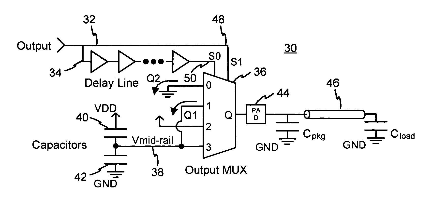
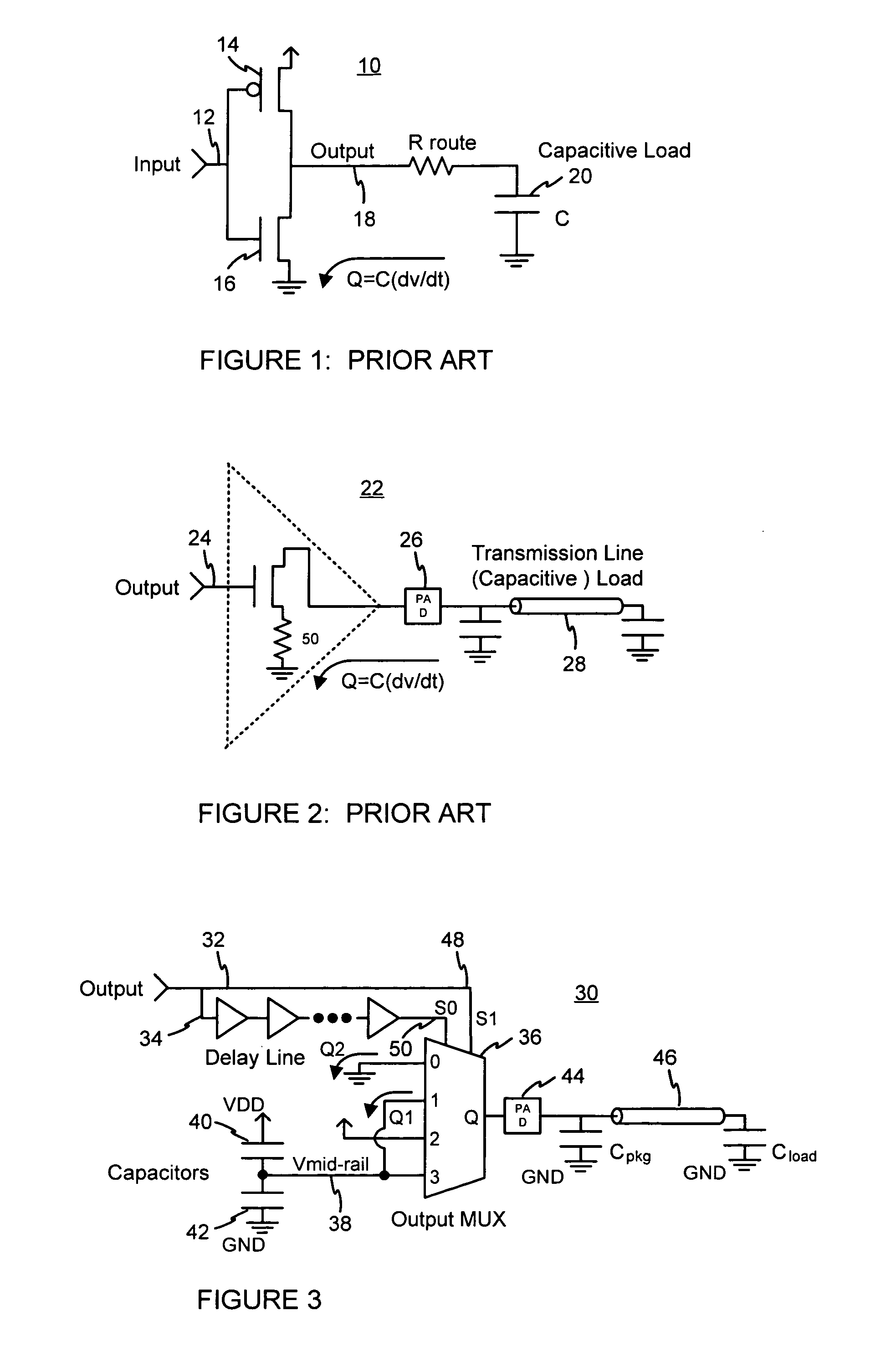
[0009]Embodiments of the present invention can significantly reduce the amount of power dissipated by CMOS circuit switching. A switching circuit and method, consistent with the present invention, use less power and can be used to slow down edge rates for lower electromagnetic interference (EMI), less power supply noise, and better signal integrity of output drivers. Embodiments of the present invention can also reduce the switching noise induced on power supplies.

[0010]A CMOS switching circuit is used to transmit data. CMOS circuits can be used for many different applications such as, for example, to perform the following functions: invert signals; repeat signals; and perform logical operations such as AND, OR, NAND, NOR, XOR, or XNOR operations. A CMOS switching circuit can also be used as, for example, an I / O buffer. The purpose of an I / O CMOS circuit (buffer) is to communicate signals from a chip embodying the circuit to the hardware outside of the chip, and from the hardware to...


PUM


Abstract

A CMOS switching circuit that includes a charge reservoir and a multiplexer connected to the charge reservoir. The multiplexer receives control signals from a delay line and a control signal line, and it delivers a switching signal to an output terminal. A first set of signals delivered to the control terminals of the multiplexer causes the charge reservoir to deliver charge to the output terminal, and a second set of signals delivered to the control terminals causes charging of the charge reservoir. With the charge reservoir, charge from falling signals is conserved and used to help rising signals at the output, reducing the power required to provide an output switching signal.

Description

BACKGROUND OF THE INVENTION[0001]Complementary Metal Oxide Semiconductor (CMOS) circuits, especially large drivers as found in Input / Output (I / O) buffer designs, are required to output high and low levels. This requires transistors to pull voltage signals “up” for high level outputs and pull signals “down” for low level outputs. Large pull-up and pull-down field effect transistors (FETs) in totem pole drivers can be required for clock drivers and to generate fast edge rates required for high bandwidth connectivity. One disadvantage of these drivers are the large amounts of alternating current (AC) switching power that they require for their operation.[0002]FIGS. 1 and 2 are circuit diagrams of prior art CMOS circuits. In FIG. 1, a circuit 10 illustrates the typical AC power consumption by a CMOS circuit. In circuit 10, an input signal on line 12 drives transistors 14 and 16. With a high input signal on line 12, transistor 14 turns off and transistor 16 turns on, driving an output lo...

Claims


Application Information

Patent Timeline
Patent Type & Authority Patents(United States)
IPC IPC(8): G06F7/38H03B1/00H03K19/173H03K3/00H03L7/06H03K19/00H03K19/0175
CPCH03K19/017545H03K19/0008
Inventor GONZALEZ, JASON
Owner AVAGO TECH INT SALES PTE LTD
Why Eureka
Try Eureka