Method of manufacturing a reflection type mask blank and method of manufacturing a reflection type mask
a technology of reflection type and manufacturing method, which is applied in the direction of photomechanical equipment, relative volume flow measurement, instruments, etc., can solve the problems of inability to achieve high-accuracy transfer, decrease in transfer accuracy (image placement error) during transfer to the wafer, and inability to manufacture high-accuracy masks. , to achieve the effect of high flatness, easy adjustment of initial stress value, and excellent smoothness
- Summary
- Abstract
- Description
- Claims
- Application Information
AI Technical Summary
Benefits of technology
Problems solved by technology
Method used
Image

Examples
example 1
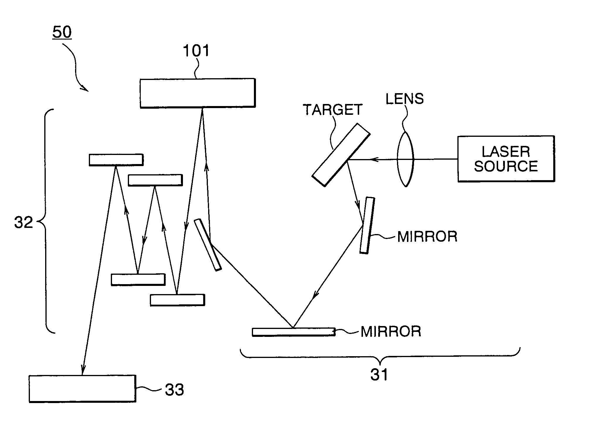
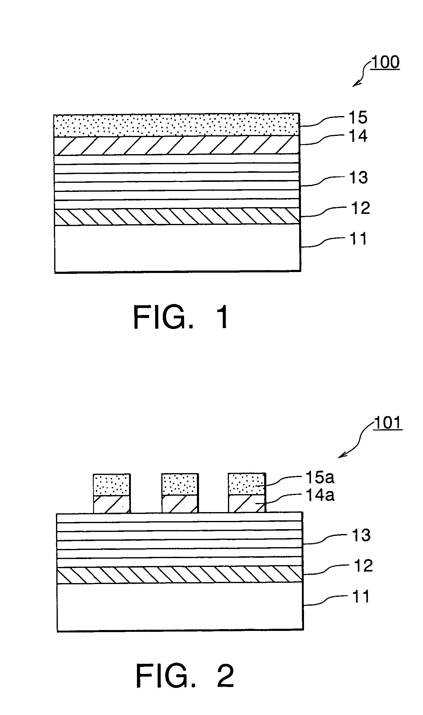
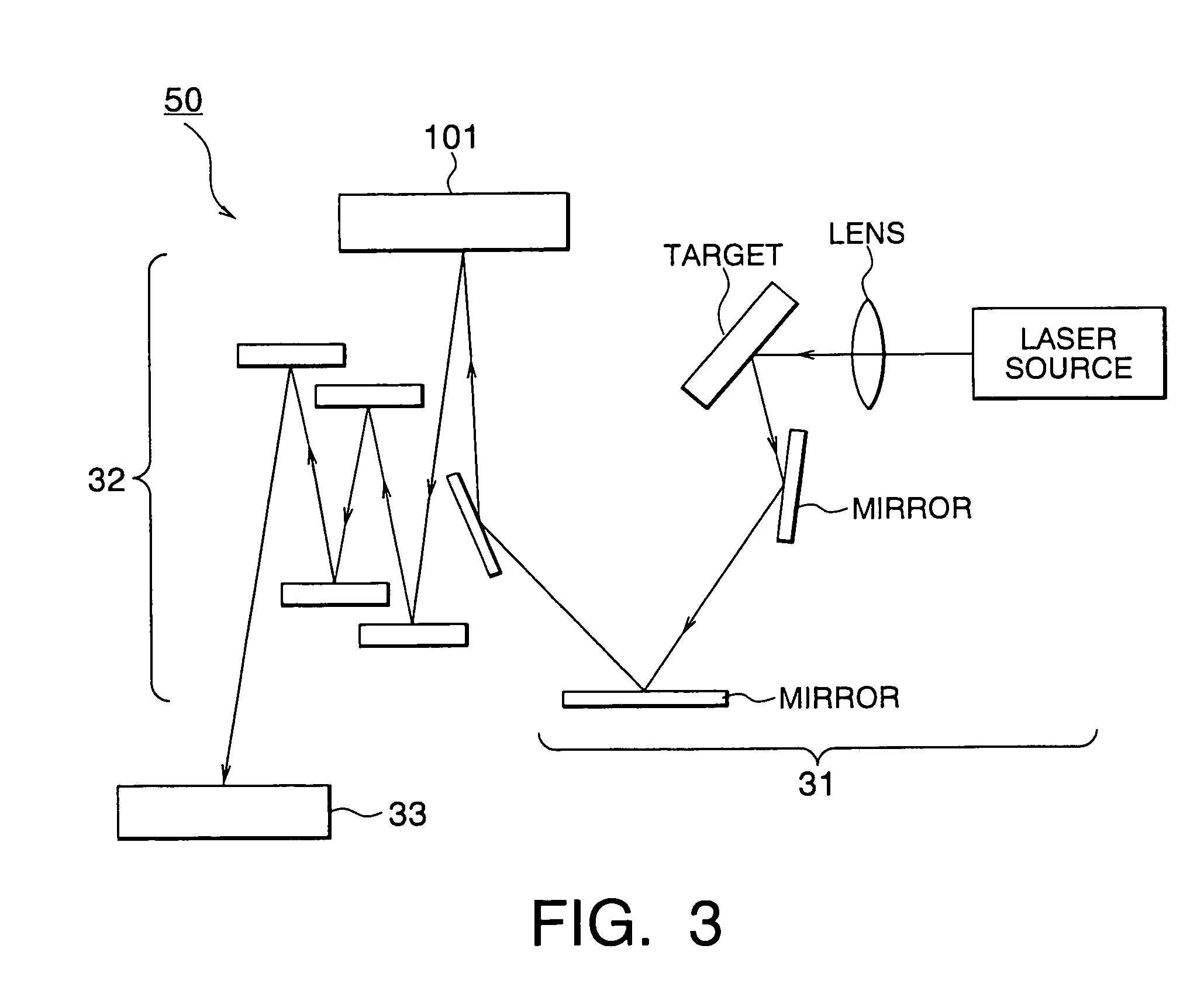
[0096]Referring to FIG. 1 and FIG. 2, description will be made of a method of manufacturing an EUV reflection type mask blank 100 and an EUV reflection type mask 101 according to this example. FIG. 1 is a sectional view of the reflection type mask blank while FIG. 2 is a sectional view of the reflection type mask.
[0097]A substrate 11 was a SiO2—TiO2 based glass substrate (outer dimension of 6 inch square, thickness of 6.3 mm). The substrate 11 had a coefficient of thermal expansion of 0.2×10⁻⁷ / ° C. and Young's modulus of 67 GPa. The glass substrate was subjected to mechanical polishing to have a smooth surface of 0.2 nmRms or less and a flatness of 100 nm or less.
[0098]At first, on the substrate 11, a film containing Ta and B was deposited to a thickness of 70 nm as a stress correction film 12. The deposition was carried out using a target containing Ta and B by the DC magnetron sputtering using Ar gas. At this time, by controlling the sputtering condition, the stress of the stress ...
example 2
[0118]In this example, the reflection type mask blank was formed in the manner similar to Example 1 except that the condition upon deposition of the stress correction film 12 was changed and the film stress initially given to the stress correction film was +50 MPa and that the heat treatment condition was set at 200° C. for 60 minutes.
[0119]The following Table 2 collectively shows the film thickness, the surface roughness, the stress before and after the heat treatment, and the flatness for each of the stress correction film and the multilayer reflection film. In this example, the stress of the substrate with the multilayer reflection film as a whole was sufficiently lowered to +66 MPa (the value scaled to the film thickness equivalent to that of the multilayer film) by the heat treatment. The
[0120]
TABLE 2Example 1 (Heating Condition 200° C., 60 min)Before HeatingAfter HeatingFilmSurfaceStress × FilmStress × FilmThicknessRoughnessStressThicknessFlatnessStressThicknessFlatnessMateria...
example 3
[0122]In this example, the stress correction film was not formed between the substrate and the multilayer reflection film but was formed on the multilayer reflection film (between the multilayer reflection film and the buffer layer). On the substrate, the multilayer reflection film and the stress correction film were successively formed. The heat treatment was carried out at 200° C. for 60 minutes after the stress correction film was formed on the multilayer reflection film. The stress correction film was formed by the use of a Ru film to the thickness of 10 nm. Except the above, the reflection type mask blank was formed in the manner similar to Example 1. The following Table 3 collectively shows the film thickness, the surface roughness, the stress before and after the heat treatment, and the flatness for each of the stress correction film and the multilayer reflection film in this example.
[0123]
TABLE 3Example 3 (Heating Condition 200° C., 60 min)In case where the stress correction...
PUM
| Property | Measurement | Unit |
|---|---|---|
| temperature | aaaaa | aaaaa |
| wavelength | aaaaa | aaaaa |
| flatness | aaaaa | aaaaa |
Abstract
Description
Claims
Application Information
 - R&D
- Intellectual Property
- Life Sciences
- Materials
- Tech Scout
- Unparalleled Data Quality
- Higher Quality Content
- 60% Fewer Hallucinations
Browse by: Latest US Patents, China's latest patents, Technical Efficacy Thesaurus, Application Domain, Technology Topic, Popular Technical Reports.
© 2025 PatSnap. All rights reserved.Legal|Privacy policy|Modern Slavery Act Transparency Statement|Sitemap|About US| Contact US: help@patsnap.com