

Sol-gel process for the manufacture of nanocomposite photoluminescent materials and materials thus produced
a photoluminescent material and nanocomposite technology, which is applied in the field ofsolgel process for the manufacture of nanocomposite photoluminescent materials and thus produced, can solve the problems of inability to exploit industrial production, high cost of reagents, and inability to meet the requirements of high-temperature photoluminescent materials,
- Summary
- Abstract
- Description
- Claims
- Application Information
AI Technical Summary
Problems solved by technology
Method used
Image

Examples
example 1
[0036]100 grams of TEOS (0.48 moles) and 8.55 grams of methyltriethoxysilane (0.048 moles) are poured under agitation in a Pyrex glass having capacity of 1 litre, obtaining a clear, single-phase liquid. Still under agitation, 300 cc of a aqueous solution of HCl of concentration 0.01 N are added; an emulsion of two non-miscible liquids is obtained. The emulsion is ultrasonically agitated during 15 minutes, by immersing in the emulsion the transducer of an ultrasonic generator mod. V 1A of the company Sonics & Materials Inc., of Newtown, Conn., USA. During this operation the alkoxides are hydrolysed and a clear, single-phase solution is obtained. This solution is subjected to low-pressure evaporation for extracting the ethanol produced during the hydrolysis. 60 grams (1 mole) of pyrogenic silica Aerosil OX-50 are then added to the solution: a suspension is obtained, that is homogenized by mechanical stirring first and then by ultrasonic agitation. An homogeneous sol of milky colour an...
example 2
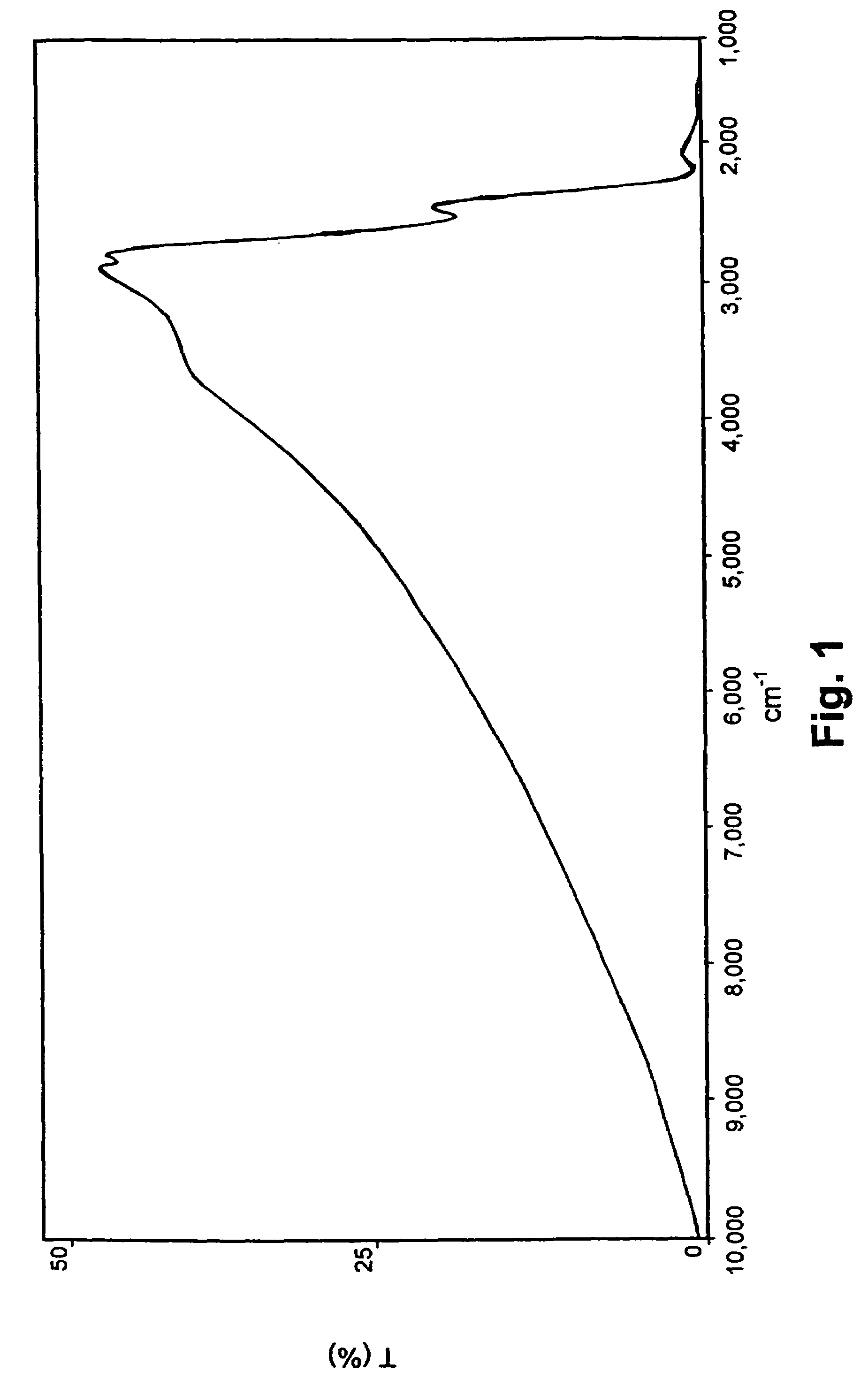
[0044]An infrared transmittance measure is carried out on a sample prepared as described in example 1 by using a FTIR analyser NICOLET NEXUS. The result of the test is the spectrum reproduced in FIG. 1, showing the transmittance of the sample, T (in %), as a function of the frequency, cm−1. The spectrum in FIG. 1 shows that the sample completely absorbs the IR radiation at frequencies higher than about 10,000 cm−1: this is a typical feature of elemental silicon. At frequencies lower than about 10,000 cm−1 the sample becomes more and more transparent to the radiation, reaching a maximum in transmittance at about 3,000 cm−1; at even lower frequencies the sample begins to absorb, reaching total absorbance around 2,000 cm−1. This latter behaviour is typical of silica.
example 3
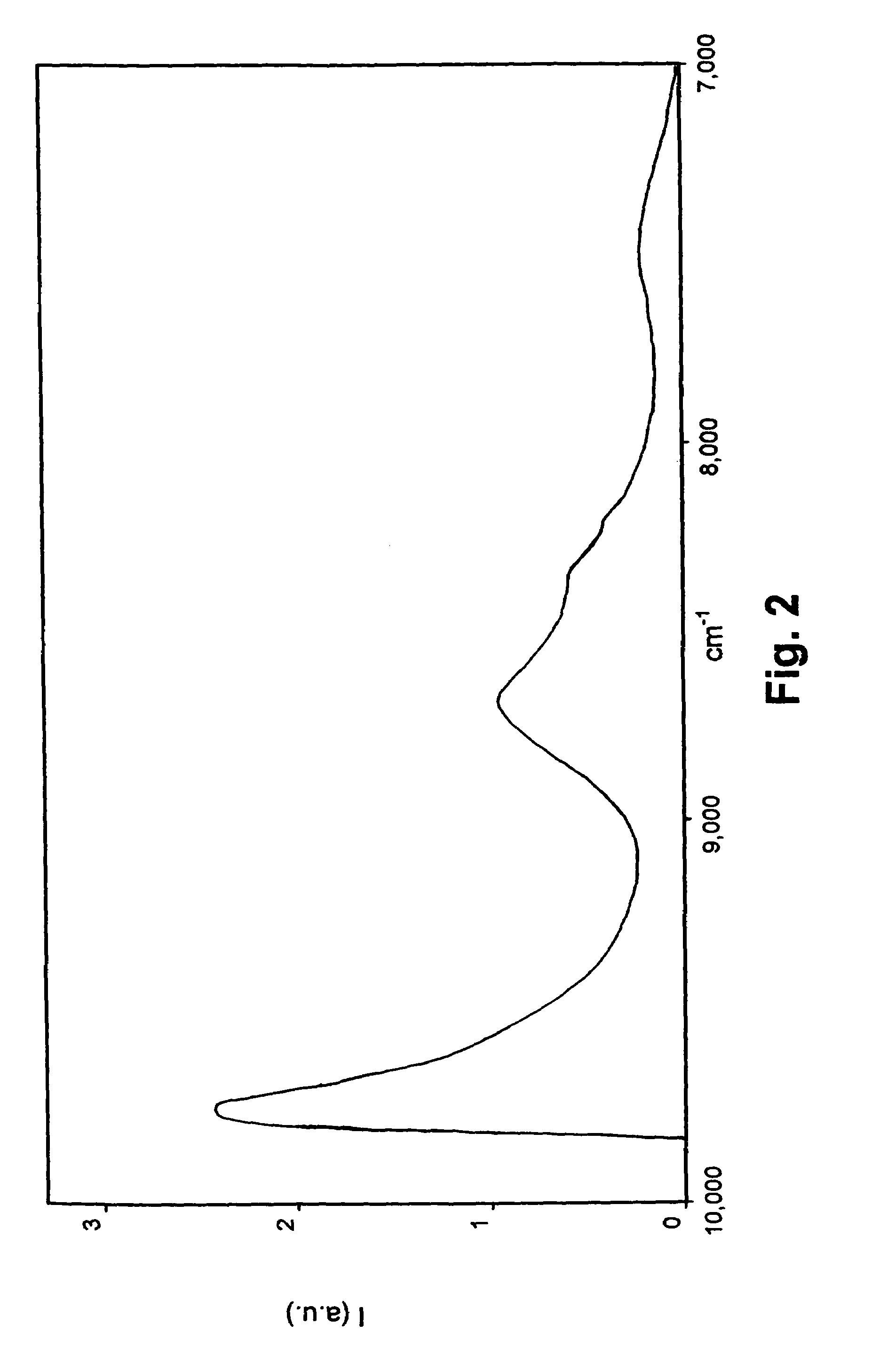
[0045]The samples produced as described in example 1 are preliminarily tested to check the presence of photoluminescence at ambient temperature. To this end, the samples are exposed to UV radiation of wavelength 365 nm obtained by filtering the radiation emitted by a mercury lamp. At visual inspection, all samples show a strong emission of deep red colour that can be attributed to an emission band centred at 780 nm, known in the literature as typical in silicon-based photoluminescent materials.
PUM
| Property | Measurement | Unit |
|---|---|---|
| Temperature | aaaaa | aaaaa |
| Temperature | aaaaa | aaaaa |
| Temperature | aaaaa | aaaaa |
Abstract
Description
Claims
Application Information