Spread spectrum clock generating circuit

a technology of generating circuit and spread spectrum, which is applied in the direction of generating/distributing signals, pulse techniques, instruments, etc., can solve the problems of increasing the period of frequency variation, affecting and increasing the accumulative delay of fundamental waves, so as to reduce the driving ability of delay circuit and reduce the circuit area. , the effect of reducing power consumption

Active Publication Date: 2006-06-13
RENESAS ELECTRONICS CORP
View PDF3 Cites 14 Cited by
  • Summary
  • Abstract
  • Description
  • Claims
  • Application Information

AI Technical Summary

Benefits of technology

[0009]It is an object of the present invention to provide a clock generating circuit having a small driving ability of a delay circuit, a reduced circuit area, reduced power consumption, a reduced delay step, and, in addition, a reduced clock jitter.
[0015]According to exemplary implementations of the present invention, a delay time of a clock signal is selected on an input side of a delay circuit and is not selected on an output side of the delay circuit, thus reducing the driving ability of the delay circuit. This enables a reduced circuit area, a reduction in power consumption, and a reduction in minimum delay step. Therefore, frequency modulation can be performed without causing a problem with jitter.

Problems solved by technology

When the EMI noise is enhanced, it generally has a negative influence on any peripheral devices.
However, as a result, a period in frequency variation is increased and accumulative delays for fundamental waves are increased.
Therefore, the analog PLL circuit is generally not suitable for use in a semiconductor integrated circuit.
This causes various problems such as, for example, an increase in circuit area, an increase in power consumption, and increased jitter due to an increased minimum delay step.
The jitter means that modulation is performed beyond frequency modulation required for EMI-noise prevention, and clock performance is thus affected.

Method used


Image

  • Spread spectrum clock generating circuit
  • Spread spectrum clock generating circuit
  • Spread spectrum clock generating circuit

Examples


first exemplary embodiment

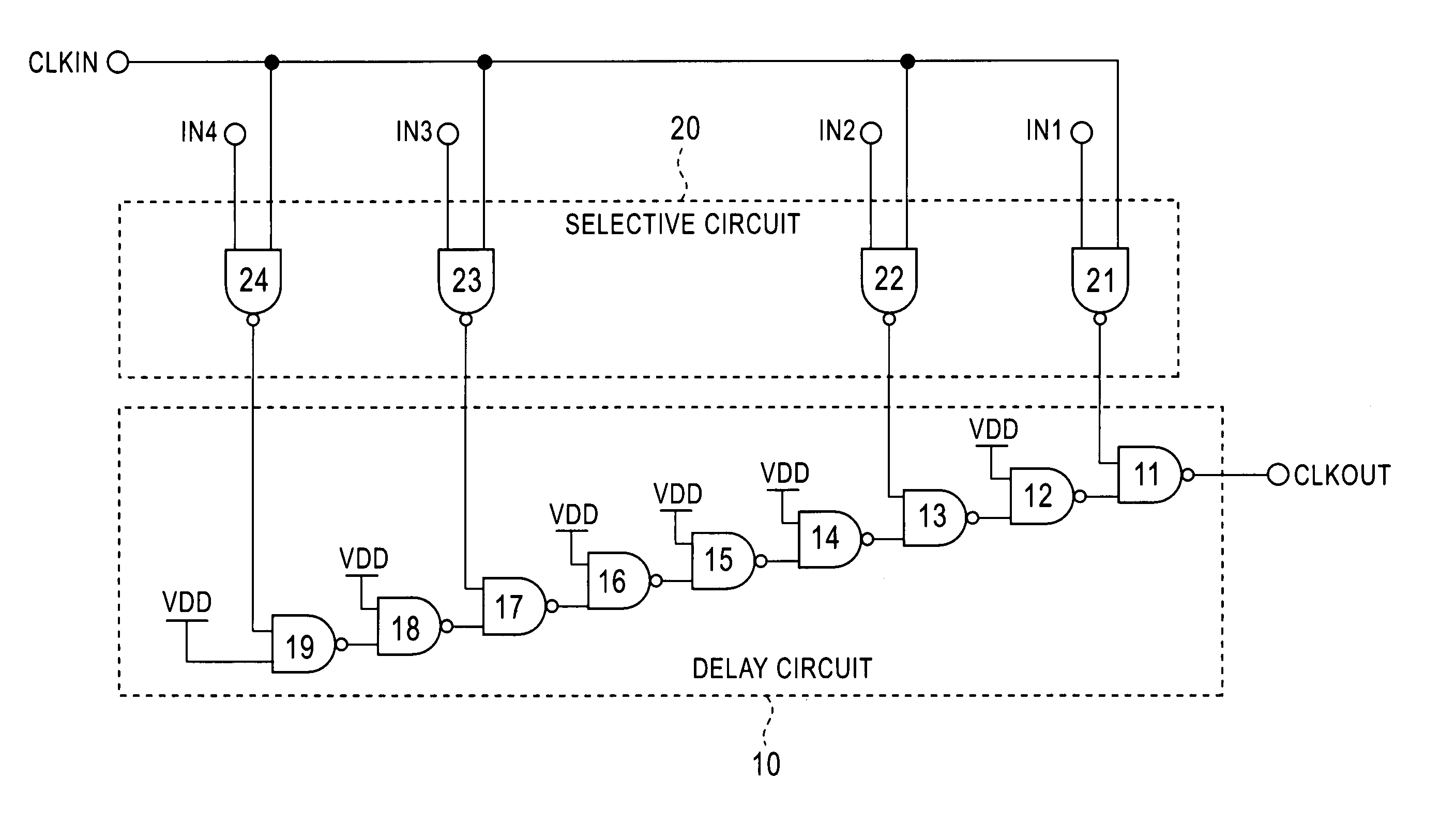
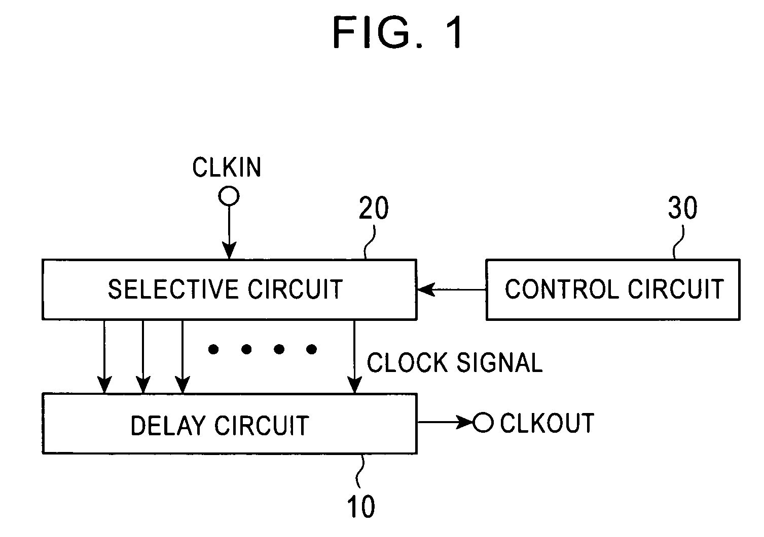
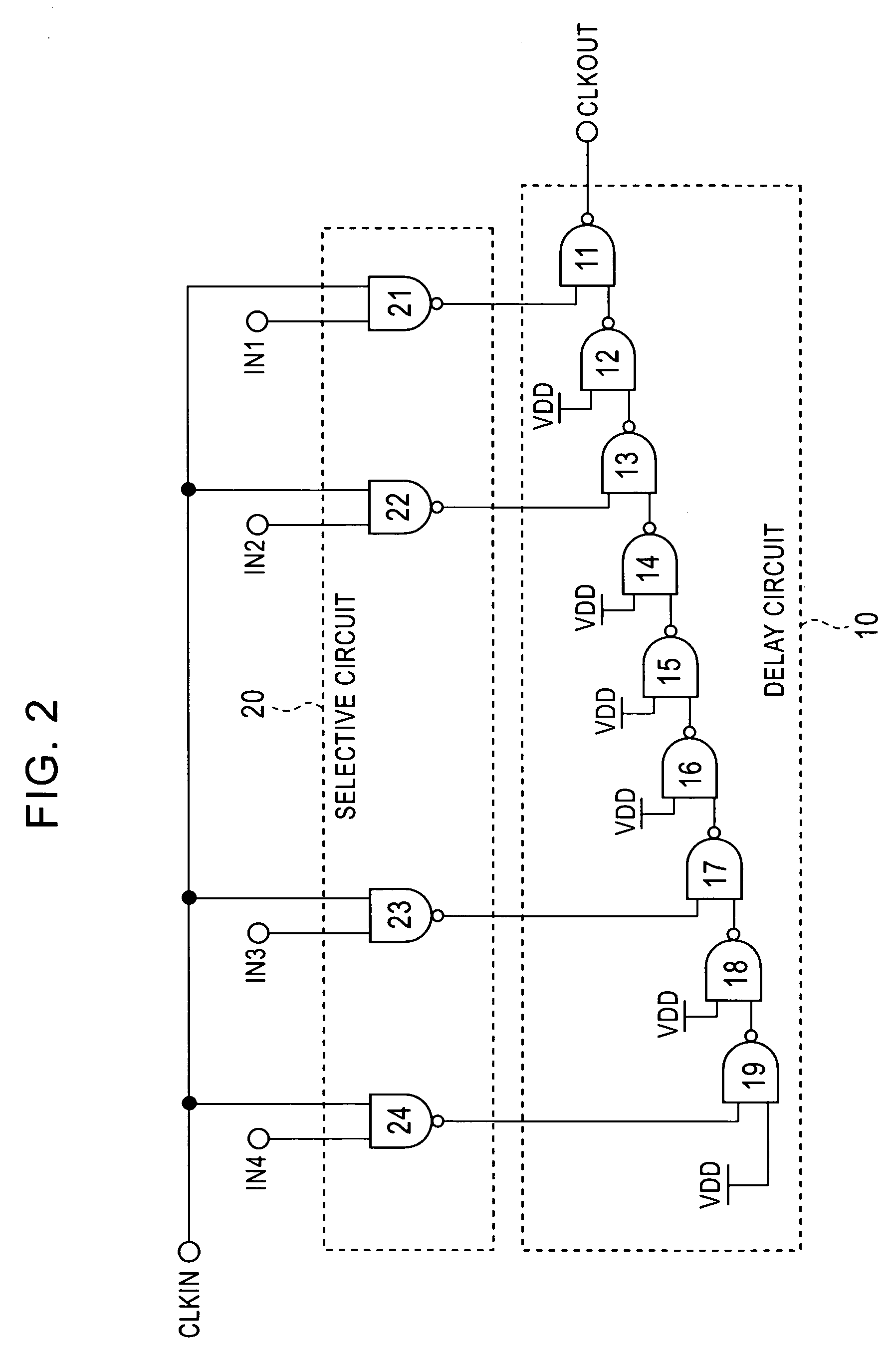
[0022]FIG. 2 is a specific exemplary block diagram showing a clock generating circuit according to a first exemplary embodiment of the present invention. A delay circuit 10 is constituted by nine two-input NAND gates 11 to 19 which are cascade-connected. A selective circuit 20 is constituted by four two-input NAND gates 21 to 24. Each output of the NAND gates 21 to 24 in the selective circuit 20 is connected to one input terminal of each of the NAND gates 11, 13, 17, and 19 in the delay circuit 10. A clock signal CLKIN is input to one input terminal of each of the NAND gates 21 to 24 in the selective circuit 20, and control signals IN1 to IN4 from a control circuit 30 (not shown in FIG. 2 and including a shift register and a binary counter) are input to the other input terminals of the NAND gates 21 to 24. In this exemplary clock generating circuit, the NAND gates 11 to 19 in the delay circuit 10 serve as delay elements, while the NAND gates 21 to 24 in the selective circuit 20 serv...

second exemplary embodiment

[0029]Although the first exemplary embodiment uses two-input NAND gates as delay elements, the delay elements are not limited to two-input NAND gates, and other logic gates such as NOR gates may be used as delay elements. When two-input NOR gates are used as delay elements and switches in the exemplary selective circuit 20, by setting one of the control signals IN1 to IN4 at the “L” level, the two-input NOR gate, to which the control signal are set to the “L” level, is opened and the input clock signal that is input to the other input terminal is inverted and output. In the first exemplary embodiment, by providing the NAND gates 21 to 24 in the selective circuit 20 with delay times equivalent to those provided by the NAND gates 11 to 19 in the delay circuit 10, a reduced number of stages of the delay elements can be achieved. However, in cases in which it is not necessary to consider a reduction in the number of stages, any delay times may be used. For example, ordinary analog switc...


PUM


Abstract

A clock generating circuit includes a delay circuit which has input terminals and which delays a signal input from each of the input terminals by a different delay time, and outputs the delayed signal from at least one output terminal, a selective circuit which receives an input clock signal and selectively outputs the clock signal to one of the input terminals of the delay circuit, and a control circuit which switches selective operations of the selective circuit. A modulated clock signal in which the period of the clock signal is increased or decreased is output from the at least one output terminal of the delay circuit such that the control circuit sequentially switches the selective operations of the selective circuit.

Description

BACKGROUND OF THE INVENTION[0001]1. Field of Invention[0002]The present invention relates to a spread spectrum clock generating circuit for reducing an electromagnetic interference (EMI) noise.[0003]2. Description of Related Art[0004]An EMI noise is an electromagnetic noise emitted from an electronic device. When the EMI noise is enhanced, it generally has a negative influence on any peripheral devices. Accordingly, for each frequency band, a regulation level is established. A common digital electronic device operates by clocks having a predetermined frequency. Normally, the clocks are in rectangular waveform, so that not only a fundamental wave noise, but also second and higher harmonics component noises are generated. In order to prevent these noises, a particular measure is generally required.[0005]Conventionally, an analog PLL (phase-locked loop) circuit is used as a spread spectrum clock generating circuit in order to prevent EMI noise. However, as a result, a period in frequen...

Claims


Application Information

Patent Timeline
Patent Type & Authority Patents(United States)
IPC IPC(8): H03K3/00G06F1/04G06F1/08H03K5/00H03K5/13H03K5/135H03K5/159H03K7/04H03L7/06H04B15/04
CPCH03K7/04H03K5/133H04B15/04H03K2005/00058H04B2215/064H04B2215/067
Inventor FUKUSHIMA, TAKAHITO
Owner RENESAS ELECTRONICS CORP
Why Eureka
Try Eureka