Unidirectional bus architecture for SoC applications

a bus and soc technology, applied in the field of flexible modular integrated circuit embodiments, can solve the problems of increasing the difficulty of a single company to provide its customers with all of the intellectual property (ip) cores, and insufficient just purchasing ips, etc., to achieve efficient integration of a variety of functional circuits

Inactive Publication Date: 2006-06-13
NETVINCI
View PDF13 Cites 63 Cited by
  • Summary
  • Abstract
  • Description
  • Claims
  • Application Information

AI Technical Summary

Benefits of technology

[0019]In sum, a system-on-chip interconnection structure and method embodiment of the present invention uses unidirectional buses only, central shared memory controllers, separate interconnects for high-speed and low-speed peripherals, zero wait-state register accesses, application-specific memory map and peripherals, application-specific test methodology, allowances for cache controllers, and fits well with standard ASIC flow and tools. The present invention enables electronics applications to be developed quickly and to be portable between silicon foundries. Additionally, the present invention provides systems that can run at higher clock speeds. These and other objects and advantages of the present invention will no doubt become obvious to those of ordinary skill in the art after having read the following detailed description of the preferred embodiments, which are illustrated in the drawings.

Problems solved by technology

As systems-on-chip (SoC) become more complex, it will be increasingly difficult for a single company to provide its customers with all of the intellectual property (IP) cores and library macrocells they require.
SoCs are reaching higher levels of integration, but their complexity is inversely proportional to the allowable time-to-market.
But just purchasing the IP is not enough.
Integrating IP in a system-on-chip is complicated, especially when components from multiple sources are involved.
At the board level, a key issue is minimizing the number of bus signals because pin and signal count translate directly into package and PCB costs.
A large number of device pins increases package footprint and reduces component density on the board.
The limited capabilities of today's logic synthesis tools directly impact embodiment time and performance and must be taken into account.
Getting the lowest possible routing overhead is of little value if the system design time balloons way out of proportion and the market window is missed.
Synthesis tools find it difficult to deal with shared tri-state signals with several drivers and receivers connected to the same trace.
Static timing analysis is awkward, and often the only way to verify timing is to use a circuit level simulator such as Spice.
All of this takes time and effort without adding real value in terms of device functionality or features.
Bus loading also limits theoretical performance and the verification problems associated with bus loading can lead to a conservative embodiment whose performance falls short of the inherent technology capabilities.
A bus designed for use on PCBs will not provide the most efficient on-chip solution.
The key issues were performance, embodiment time reduction, ease of use, power consumption and silicon efficiency.

Method used


Image

  • Unidirectional bus architecture for SoC applications
  • Unidirectional bus architecture for SoC applications
  • Unidirectional bus architecture for SoC applications

Examples


Embodiment Construction

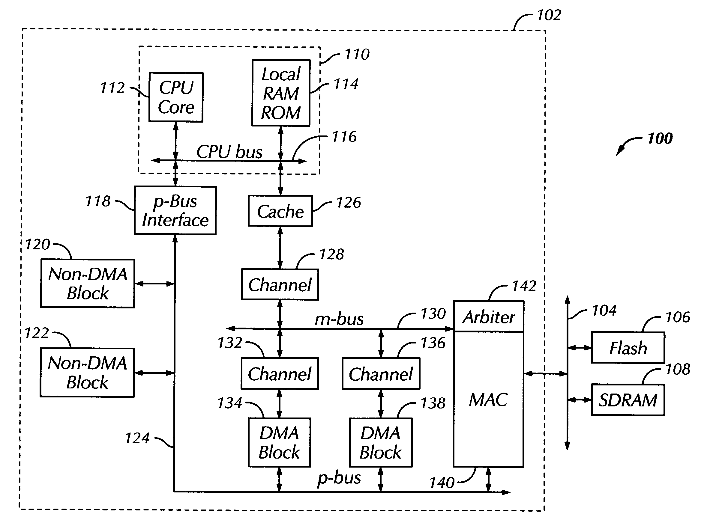
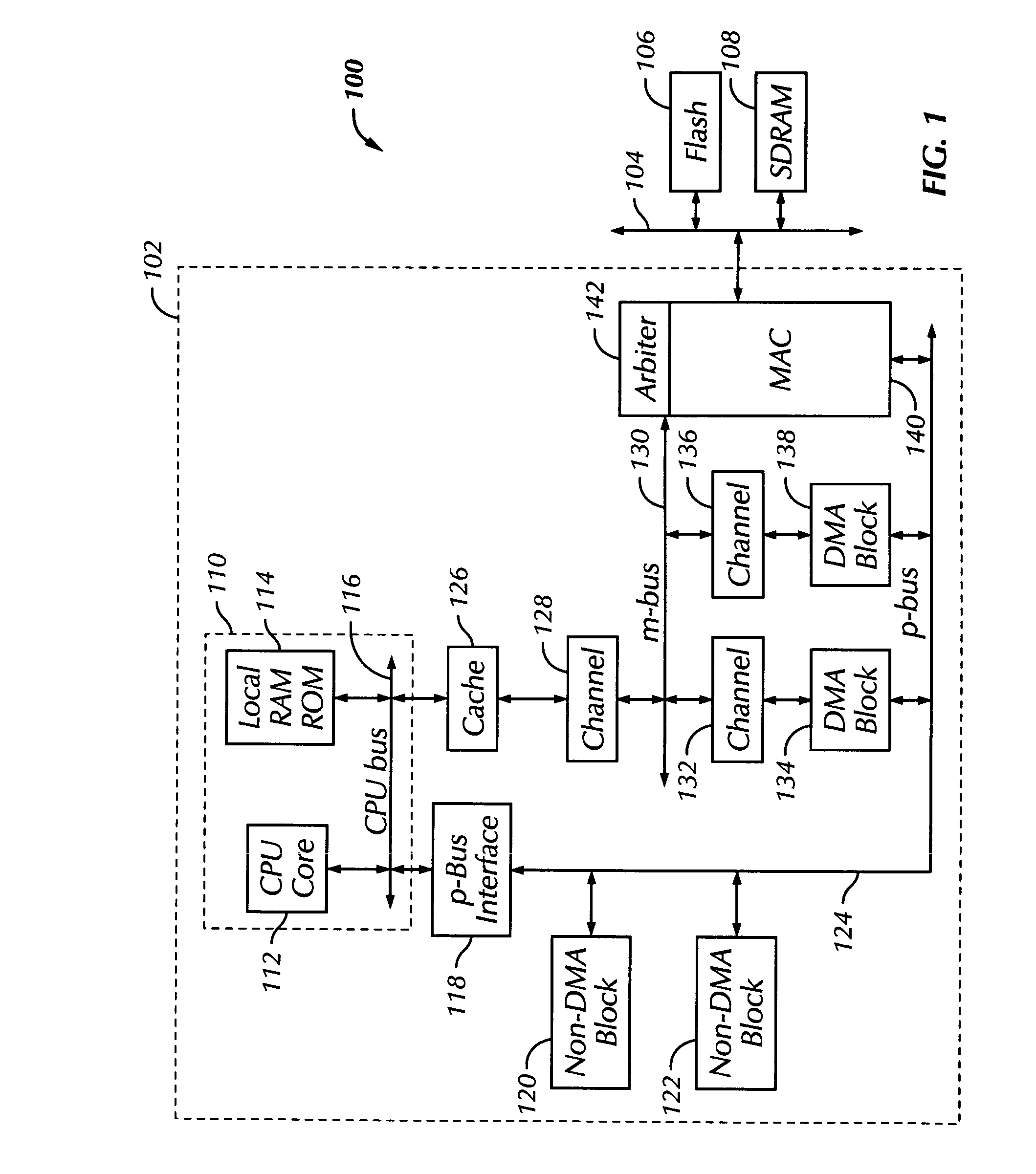
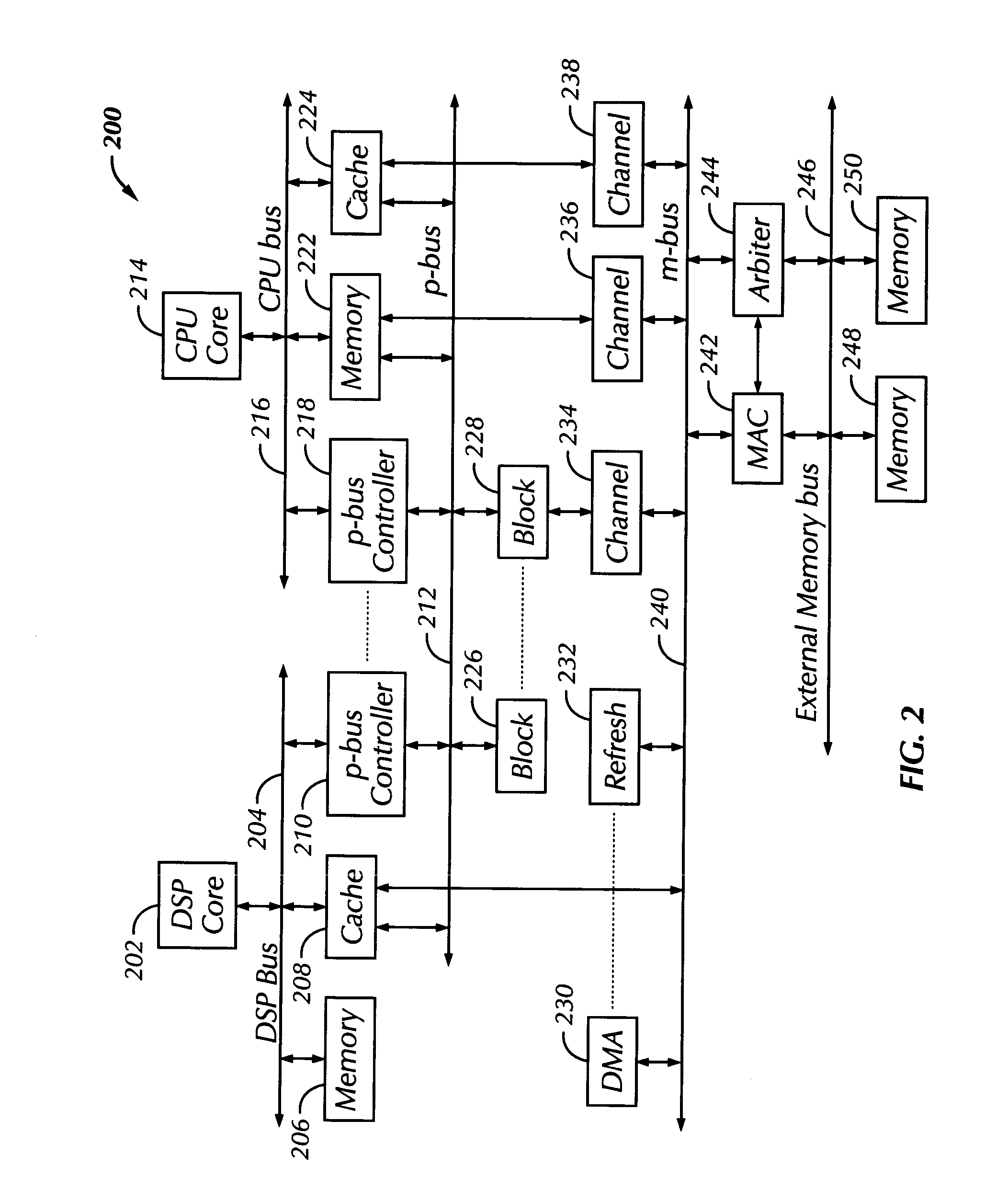
[0049]The present invention is a system-on-chip interconnection structure and method that enables the efficient on-chip integration of a variety of functional circuits and peripherals. The present invention provides an on-chip interconnect architecture that standardizes how systems-on-chip are fabricated on silicon semiconductor integrated circuit chips. This disclosure describes numerous specific details that include specific structures, circuits, and logic functions in order to provide a thorough understanding of the present invention. One skilled in the art will appreciate that one may practice the present invention without these specific details.

[0050]FIG. 1 illustrates an on-chip interconnect architecture embodiment of the present invention for system-on-chip integration, and is referred to by the general reference numeral 100. The system-on-chip interconnect architecture 100 comprises a single semiconductor chip 102 that may be externally interfaced to a shared memory bus 104 ...


PUM


Abstract

The System-on-Chip apparatus and integration methodology disclosed includes a single semiconductor integrated circuit having one or more processor subsystems, one or more DMA-type peripherals, and a Memory Access Controller (MAC) on a first internal unidirectional bus. The first internal unidirectional bus controls transactions between the processor subsystem(s) and the DMA peripheral(s) using a Memory Access Controller (MAC) and unidirectional, positive-edge clocked address and transaction control signals. The first internal unidirectional bus can support burst operation, variable-speed pipelined memory transactions, and hidden arbitration. The SoC may include a second internal unidirectional bus that controls transactions between the processor subsystem(s) and non-DMA peripherals. The second internal unidirectional bus controls transactions between the processor subsystem(s) and the non-DMA peripheral(s) using unidirectional address and transaction control signals. Peripherals may be synchronous or asynchronous to their respective buses.

Description

CROSS REFERENCE TO RELATED APPLICATIONS[0001]This application is a continuation of U.S. patent application Ser. No. 09 / 565,282, filed May 2, 2000 (May 2, 2000) now U.S Pat. No 6,601,126, which is incorporated by reference for all purposes into this specification.[0002]Additionally, this application claims the benefits of the earlier filed U.S. Provisional App. Ser. No. 60 / 176,921 filed Jan. 20, 2000 (Jan, 20, 2000), which is incorporated by reference for all purposes into this specification.BACKGROUND OF THE INVENTION[0003]1. Field of the Invention[0004]The present invention relates generally to flexible modular integrated circuit embodiments, and more specifically to a structured framework for constructing and interfacing variable mixtures of computer processors, memories, peripherals, and other functional modules on a single semiconductor integrated circuit.[0005]2. Description of the Related Art[0006]As systems-on-chip (SoC) become more complex, it will be increasingly difficult ...

Claims


Application Information

Patent Timeline
Patent Type & Authority Patents(United States)
IPC IPC(8): G06F13/00G06F15/78G11C7/00
CPCG06F15/7832Y02B60/1225Y02B60/1207Y02D10/00
Inventor ZAIDI, S. JAUHER A.OU, MICHAELADAMS, LYLE E.RAMLAOUI, HUSSAM I.MILLS, BILLY D.BHAGAT, ROBIN
Owner NETVINCI
Why Eureka
Try Eureka