Compiler synchronized multi-processor programmable logic device with direct transfer of computation results among processors

a programmable logic and processor technology, applied in computation using denominational number representation, instruments, architectures with multiple processing units, etc., can solve the problems of increasing the place and route time of such devices, increasing the complexity of layout analysis, and requiring cumbersome and laborious critical path timing analysis of routed designs. , to achieve the effect of quick and efficient processing of system level designs and better utilization of silicon surface area

Inactive Publication Date: 2005-07-05
HYDUKE STANLEY M
View PDF6 Cites 10 Cited by
  • Summary
  • Abstract
  • Description
  • Claims
  • Application Information

AI Technical Summary

Benefits of technology

[0019]The purpose of this invention is to better utilize the silicon surface area by using highly regular memory structure for logic applications instead of such cells as gates and flip-flops. Sequencers are logic processors that do not have jump, branch or similar instructions that change the order of instruction execution. This invention describes how a set of synchronized sequencers can be used for quick and efficient processing of system level designs.

Problems solved by technology

For example, the place and route time for such devices increases rather exponentially.
The present technologies also require cumbersome and labor intensive critical path timing analysis of the routed designs.
New physical phenomena are playing larger role at higher cell densities, making the layout analysis continuously more complex.
However, such incremental silicon compilation would require a substantial human effort and involvement, which will slow even more the design process.
This makes the design more complex and lowers the effective utilization of silicon surface area.
However, since there is no other good way to test the silicon, this process is widely applied to ASIC devices in excess of 100,000 gates.
This lowers the effective utilization of the silicon.
The current technologies dissipate a large amount of heat because all circuits operate in parallel.
This limits the design size that can be placed on the silicon.
The current silicon production growth outstrips design tool capabilities by a large margin.
While the silicon technologies allow building devices with tens of millions of transistors, the current commercial design tools limit that number to around ten million transistors.
Because of that, the design tools are a major drag on further spread of silicon device applications.
However, the fault is not with the design tools but with the way digital circuits are implemented in silicon.
The currently used silicon architectures make design tools unnecessarily slow, cumbersome and difficult to use.

Method used


Image

  • Compiler synchronized multi-processor programmable logic device with direct transfer of computation results among processors
  • Compiler synchronized multi-processor programmable logic device with direct transfer of computation results among processors
  • Compiler synchronized multi-processor programmable logic device with direct transfer of computation results among processors

Examples


Embodiment Construction

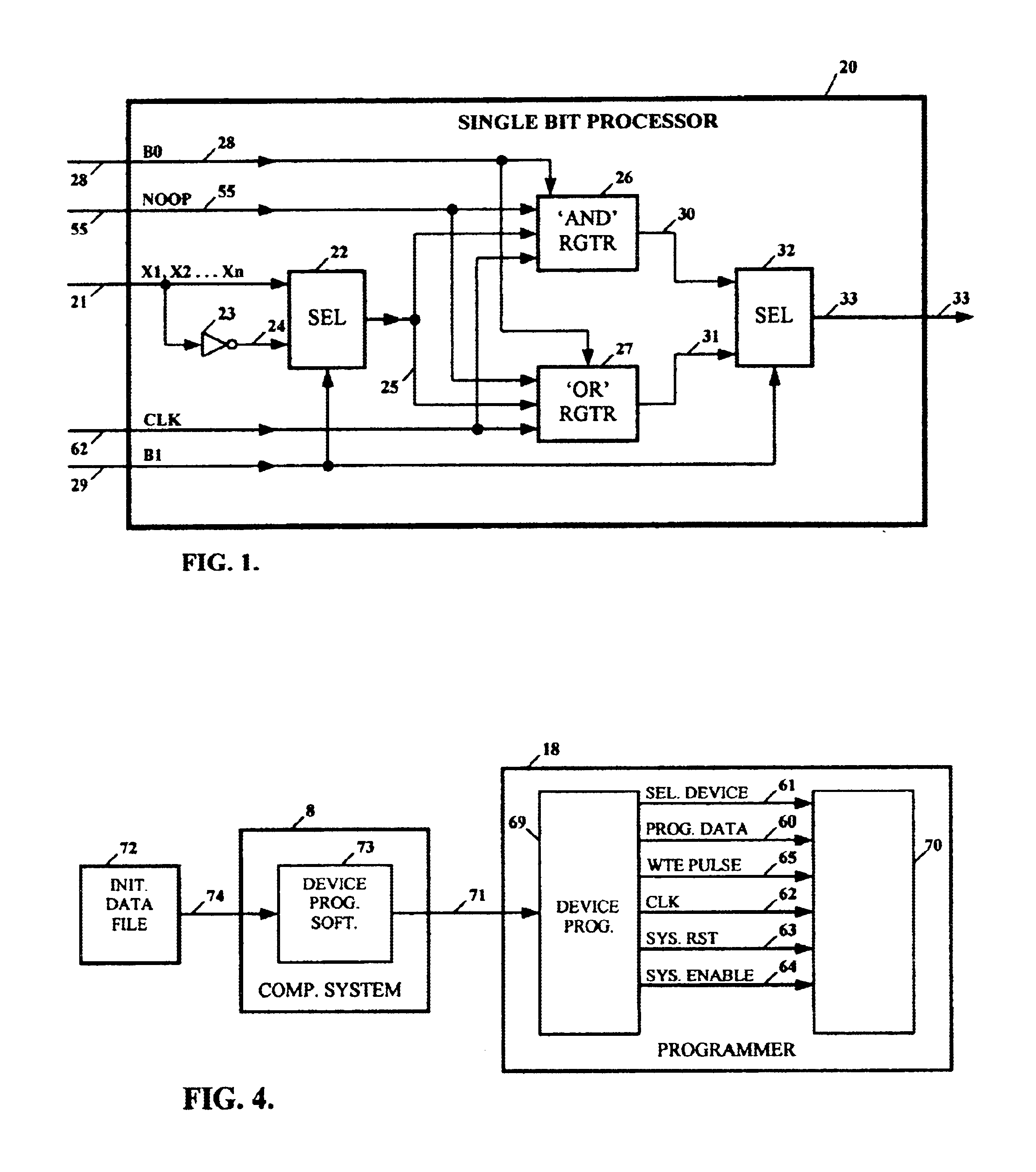
[0033]A single bit processor embodiment is illustrated in FIG. 1. This embodiment facilitates Reverse Polish Notation (RPN) machine instruction execution. Processor 20 is based on two (2) concurrent operations that are performed on all input variables in parallel. They are shown in FIG. 1 by way of an example as AND register 26 and OR register 27. Since processor 20 allows an inversion operation by means of inverter 23, the presence of both registers 26 and 27 is not mandatory to execute logic equations, because de Morgan theorem allows conversion of AND operations into OR operations and vice versa by using the inverter 23. It will be within the scope of the invention to replace either the AND register 26 or the OR register 27 by a block performing an XOR or other logic operation.

[0034]AND register 26 is set to logical one (1) at the beginning of each logic equation execution. The first zero (0) will reset the register 26 to zero (0) and will keep it at zero (0) independent of the f...


PUM


Abstract

A system for designing and implementing digital integrated circuits utilizing a set of synchronized sequencers that permit quick and efficient parallel processing of system level designs. The system and method converts digital schematics and hardware description language (HDL) based designs into a set of logic equations and single bit arithmetic-logic operations executed by a set of parallel operating sequencers. The system includes software for converting netlists and HDL designs into Boolean logic equations, and a compiler for distributing these logic equations between multiple sequencers. Each sequencer is comprised of a logic processor and the associated program memory for storing the executable code of the assigned Boolean logic equations and data memory for storing the results of processing of logic equations. To synchronize execution of logic equations by multiple sequencers, all program memories are addressed by one common address register. The processing of logic equations is arranged in such a manner that their outputs can be read by synchronized read instructions in the interconnected sequencers, eliminating any need for control signals.

Description

CROSS-REFERENCE TO RELATED APPLICATIONS[0001]This application is a Continuation of U.S. patent application Ser. No. 09 / 512,091, filed Feb. 24, 2000 now U.S. Pat. No. 6,578,133.FIELD OF THE INVENTION[0002]The present invention relates to digital circuit implementation and more particularly relates to a new silicon device architecture for quick and efficient design and implementation of digital integrated circuits.BACKGROUND OF THE INVENTION[0003]The art of digital integrated circuit implementation in silicon is well established. There are numerous technologies such as Application Specific Integrated Circuits (ASIC), Field Programmable Gate Arrays (FPGAs) and Complex Programmable Logic Devices (CPLD) which implement digital circuits by means of interconnected cells such as gates, flip-flops and other digital elements. The biggest advantage of these technologies is fast operation caused by parallel activity of all digital elements.[0004]However, the present technologies also have a num...

Claims


Application Information

Patent Timeline
Patent Type & Authority Patents(United States)
IPC IPC(8): G06F17/50G06F15/76G06F15/80
CPCG06F15/8007G06F17/5022G06F17/5045G06F30/30G06F30/33G06F15/16G06F30/3308
Inventor HYDUKE, STANLEY M.
Owner HYDUKE STANLEY M
Why Eureka
Try Eureka