Reflecting device for electromagnetic waves

a technology of electromagnetic waves and reflectors, which is applied in the direction of instruments, lighting and heating devices, photomechanical devices, etc., can solve the problems of impaired surface roughness achieved beforehand by superpolishing methods, and achieve the effect of improving surface quality with regard to hsfr and high reflectivity

Inactive Publication Date: 2006-07-18
CARL ZEISS SMT GMBH
View PDF9 Cites 6 Cited by
  • Summary
  • Abstract
  • Description
  • Claims
  • Application Information

AI Technical Summary

Benefits of technology

[0018]In an intermediate layer made of silicon, what is additionally achieved, as shown in experiments, is that the surface quality with regard to HSFR can be improved again relative to the surface quality of the original surface, lying below the intermediate layer, by means of the beam processing of silicon. It is thus possible to achieve HSFR qualities which lie significantly below 0.1 nm rms. Such devices for reflecting electromagnetic waves are thus highly suitable even for electromagnetic waves having a wavelength in the range from 10 to 20 nm, in connection with the multi-layer reflection layers known per se, for achieving a very high reflectivity.

Problems solved by technology

This is because the inventors have found that during the processing of such materials with vanishing thermal expansion, which, according to the currently known prior art, predominantly comprise, at least in the microscopic region, two or multiphase mixtures, the individual constituents are removed to different degrees by beam processing methods, so that the surface roughness achieved beforehand by means of superpolishing methods is impaired again after the beam processing.

Method used


Image

  • Reflecting device for electromagnetic waves
  • Reflecting device for electromagnetic waves

Examples


Embodiment Construction

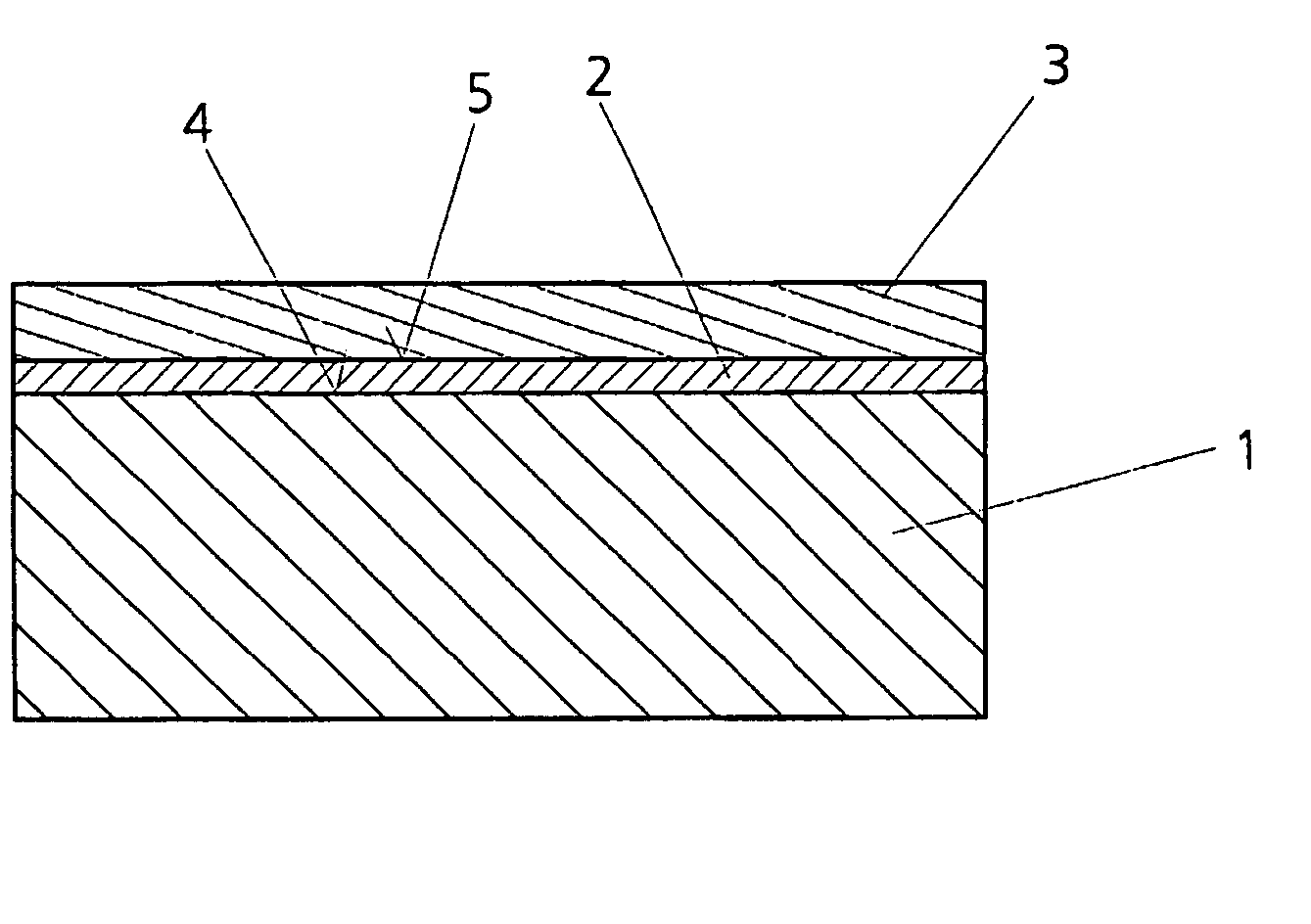
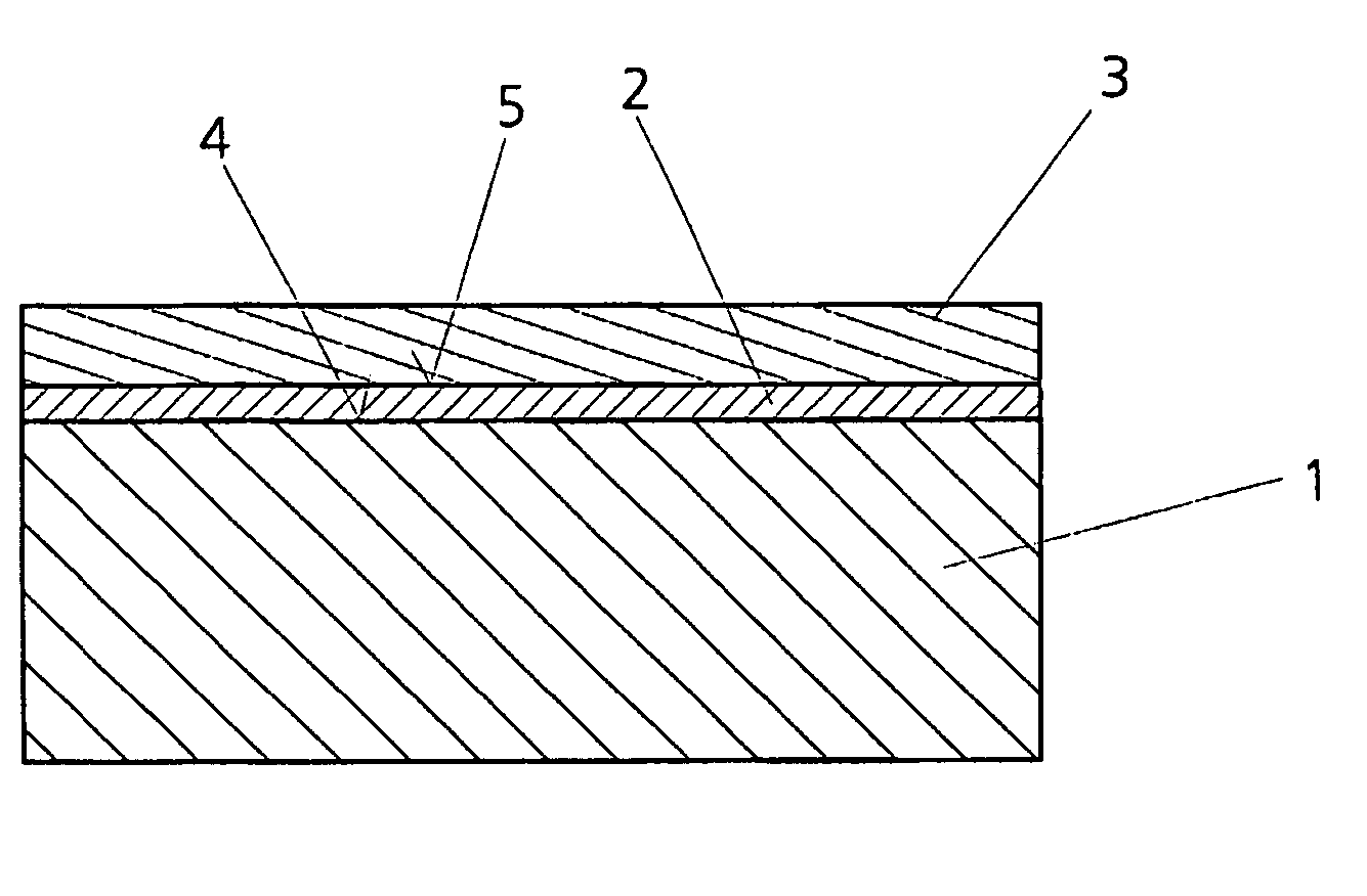
[0027]In addition to these requirements with regard to the thermal expansion, the mirror carrier 1 must have, at its surface 4 which later carries the multilayer layer 3, very stringent requirements with regard to the figure, which is responsible for the imaging quality, with regard to the MSFR (mid spatial frequency roughness), which is responsible for scattering effects and contrast, and with regard to the HSFR (high spatial frequency roughness), which is responsible for the reflectivity. In order to be able to operate in the range of wavelengths below 200 nm, for example with X-ray waves in the range of λ=10–20 nm, for example the value of the HSFR must be significantly less than 0.5 nm rms, preferably 0.2 nm rms, particularly preferably 0.1 nm rms.

[0028]Conventional superpolishing methods are perfectly capable of obtaining such surface qualities with regard to HSFR. In the case of mirrors, in particular in the case of aspherical mirrors, the figure and longer-wave ranges of the ...


PUM

PropertyMeasurementUnit
wavelength rangeaaaaaaaaaa
thicknessaaaaaaaaaa
thicknessaaaaaaaaaa

Abstract

A device serves for reflecting electromagnetic waves, in particular in a length range less than 200 nm. It has a mirror carrier made of a material with at least approximately vanishing thermal expansion and at least one reflective layer applied on said mirror carrier. An intermediate layer made of a material which is formed such that its surface roughness is not significantly increased after beam processing methods is fitted between the mirror carrier and the reflective layer.

Description

BACKGROUND OF THE INVENTION[0001]1. Field of the Invention[0002]The present invention relates to a reflecting device for electromagnetic waves, comprising a mirror carrier made of a material with at least approximately vanishing thermal expansion and at least one reflective layer applied on said mirror carrier.[0003]Moreover, the invention relates to a method for producing such a device for reflecting electromagnetic waves.[0004]More specifically, the invention relates to electromagnetic waves in a wavelength range less than 200 nm.[0005]2. Description of the Related Art[0006]DE 198 30 449 A1 discloses a mirror substrate which comprises crystal and is provided with an amorphous layer of the order of magnitude of 1 to 100 μm, which allows a much higher polishing quality than the mirror substrate itself. In this case, the use of such a mirror is provided in EUV projection exposure installations.[0007]In general, it is known that mirrors in EUV installations, for example EUV lithograph...

Claims


Application Information

Patent Timeline
Patent Type & Authority Patents(United States)
IPC IPC(8): G02B5/08G03F1/24G03F7/20G21K1/06
CPCB82Y10/00B82Y40/00G21K1/06G03F7/2008G03F7/70958G03F1/24
Inventor WEISER, MARTINDINGER, UDOSTACKLIES, SIEGFRIEDHAIDL, MARKUS
Owner CARL ZEISS SMT GMBH
Why Eureka
Try Eureka