Enhanced photodetector

a photodetector and enhanced technology, applied in the field of semiconductor-based photodetectors, can solve the problems of reducing absorption and lower responsivity, increasing the transit time of carriers, and diodes with a very small junction capacitance and corresponding fast response, so as to increase the speed of pin diodes, reduce the resistance, and reduce the resistance

Inactive Publication Date: 2006-07-18
MACOM TECH SOLUTIONS HLDG INC
View PDF30 Cites 4 Cited by
  • Summary
  • Abstract
  • Description
  • Claims
  • Application Information

AI Technical Summary

Benefits of technology

[0003]There is a well-known tradeoff between high speed and sensitivity in a photodetector. High bandwidth signal detection requires a short transit time of the carriers and thus a thin absorption layer. However, the geometrical constraints on the absorption layer thickness results in a reduced absorption and lower responsivity.
[0005]In a PIN diode, the depletion layer extends into each side of junction by a distance that is inversely proportional to the doping concentration. Thus, the p-i depletion layer extends well into the intrinsic material, as does the depletion layer of the i-n junction. Accordingly, a PIN diode functions like a p-n junction with a depletion layer that encompasses the entirety of the intrinsic material. The primary advantages inherent to this structure are twofold. First, the addition of the intrinsic layer permits a fractional increase in the amount of light to be captured by the diode. Secondly, due to the extended depletion layer, the PIN diode has a very small junction capacitance and corresponding fast response.
[0006]Most attempts at increasing the speed of PIN diodes have focused on reducing the capacitance at the junction. At least one proposed design has included an undoped drift region for this purpose, effectively increasing the size of the intrinsic portion of the diode. Although this solution is suitable for decreasing the junction capacitance, it unfortunately increases the transit time for the carriers and thus reduces the response time of the photodetector. As such, there is a need in the art for an improved photodetector that strikes the proper balance between capacitance and response time, while increasing the responsivity of the device.
[0007]Accordingly, the present invention includes a photodiode having a first p-type semiconductor layer and an n-type semiconductor layer coupled by a second p-type semiconductor layer. The second p-type semiconductor layer has graded doping along the path of the carriers. In particular, the doping is concentration graded from a high value near the anode to a lower p concentration towards the cathode. By grading the doping in this way, an increase in absorption is achieved, improving the responsivity of the device. Although this doping increases the capacitance relative to an intrinsic semiconductor of the same thickness, the pseudo electric field that is created by the graded doping gives the electrons a very high velocity which more than compensates for this increased capacitance. Further embodiments and advantages of the present invention are discussed below with reference to the figures.BRIEF DESCRIPTION OF THE DRAWINGS

Problems solved by technology

However, the geometrical constraints on the absorption layer thickness results in a reduced absorption and lower responsivity.
Secondly, due to the extended depletion layer, the PIN diode has a very small junction capacitance and corresponding fast response.
Although this solution is suitable for decreasing the junction capacitance, it unfortunately increases the transit time for the carriers and thus reduces the response time of the photodetector.

Method used


Image

  • Enhanced photodetector
  • Enhanced photodetector
  • Enhanced photodetector

Examples


Embodiment Construction

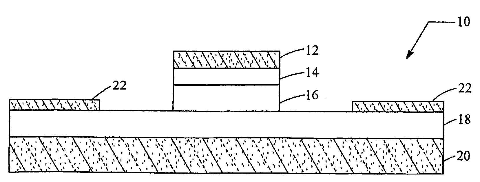
[0012]In accordance with a preferred embodiment of the present invention, an epitaxial structure is provided for photoconductive purposes. The photoconductive structure is a modified PIN diode that is optimized for increased performance through an enhanced layer having a graded doping concentration. The particulars of the structure and method of manufacture of the present invention are discussed further herein.

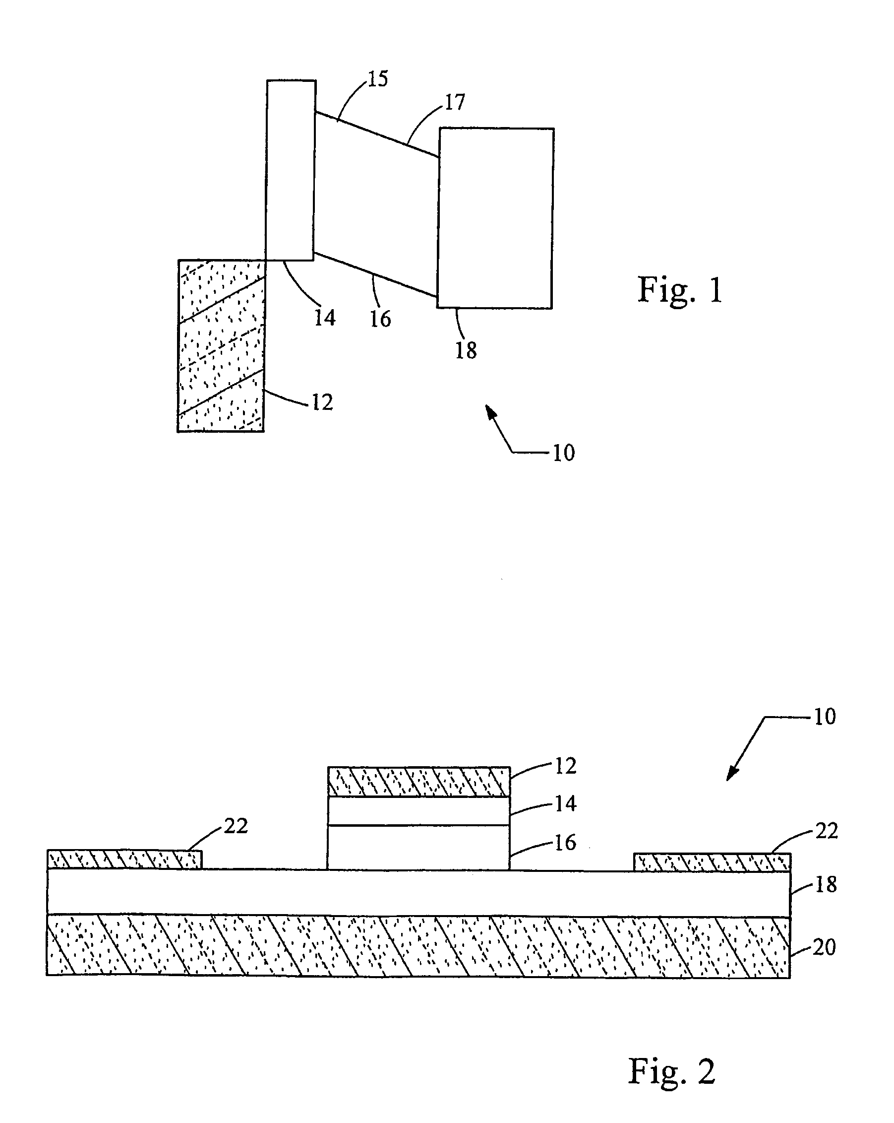
[0013]Referring to FIG. 1, an energy band diagram of a PIN photodiode 10 shows the relative energy levels of the semiconductor materials that form the photodiode 10. In particular, the photodiode 10 is comprised of a group of semiconductor materials, including a first p-type semiconductor layer 14, a second p-type semiconductor layer 16, and an n-type semiconductor layer 18. An anode layer 12 is shown adjacent to the first p-type semiconductor layer 14 to collect holes.

[0014]The first p-type semiconductor layer 14 is selected from a group comprising tertiary semiconductors, or...


PUM


Abstract

The present invention includes a photodiode having a first p-type semiconductor layer and an n-type semiconductor layer coupled by a second p-type semiconductor layer. The second p-type semiconductor layer has graded doping along the path of the carriers. In particular, the doping is concentration graded from a high value near the anode to a lower p concentration towards the cathode. By grading the doping in this way, an increase in absorption is achieved, improving the responsivity of the device. Although this doping increases the capacitance relative to an intrinsic semiconductor of the same thickness, the pseudo electric field that is created by the graded doping gives the electrons a very high velocity which more than compensates for this increased capacitance.

Description

CROSS-REFERENCE TO RELATED APPLICATIONS[0001]This application is a filing under 35 U.S.C. 371, which claims priority to International Application Serial No. PCT / US03 / 03181, filed Feb. 3, 2003, which claims the benefit of U.S. Provisional Application No. 60 / 353,849, filed Feb. 1, 2002.FIELD OF THE INVENTION[0002]The present invention relates to a semiconductor-based photodetector, and in particular to a high-speed, broad bandwidth photodetector having enhanced absorption characteristics.BACKGROUND AND SUMMARY OF THE INVENTION[0003]There is a well-known tradeoff between high speed and sensitivity in a photodetector. High bandwidth signal detection requires a short transit time of the carriers and thus a thin absorption layer. However, the geometrical constraints on the absorption layer thickness results in a reduced absorption and lower responsivity.[0004]One type of semiconductor-based photodetector is termed a p-i-n junction diode, or a PIN diode. This type of structure is generally...

Claims


Application Information

Patent Timeline
Patent Type & Authority Patents(United States)
IPC IPC(8): H01L31/109H01L31/10H01LH01L21/00H01L29/732H01L31/00H01L31/0304H01L31/0328H01L31/075H01L31/103
CPCH01L31/03042H01L31/03046H01L31/1035H01L31/105H01L31/102Y02E10/544Y02E10/548H01L31/075H01L31/10H01L31/103
Inventor KO, CHENG C.LEVINE, BARRY
Owner MACOM TECH SOLUTIONS HLDG INC
Why Eureka
Try Eureka