
Method of fabricating patterned polymer film with nanometer scale

Inactive Publication Date: 2006-07-25
KOREA ADVANCED INST OF SCI & TECH
View PDF8 Cites 41 Cited by
  • Summary
  • Abstract
  • Description
  • Claims
  • Application Information

AI Technical Summary

Benefits of technology

[0010]Therefore, it is an object of the present invention to alleviate the problems encountered in the related art and to provide a method of fabricating a patterned polymer film with nanometer scale, characterized in that polymer patterns having nanometer sized line widths therebetween (which are difficult to realize by a photolithography or electron beam process) can be rapidly and inexpensively fabricated at desired locations by use of a self-assembling process and a soft lithography process.

Problems solved by technology

However, when using a conventional semiconductor photolithography process, it is difficult to fabricate patterns having line widths of 100 nanometer or less, because of the limitation of the photolithographic resolution.
Although these methods result in finer line widths and higher resolution compared to photolithography, they require expensive equipment and long processing periods.
However, conventional methods of forming the nano-patterns have a problem in that desired patterns cannot be prepared at desired positions by only self-assembly (see Chem. Mater. 11:2322 (1999); Science 287:2240 (2000); Nature 414:293 (2001); Adv. Mater. 14:930 (2002); Chem. Commun. 982 (2003); Adv. Mater. 15:703 (2003); Langmuir 12:4033 (1996); Appl. Phys. Lett. 78:2273 (2001)).

Method used


Image

  • Method of fabricating patterned polymer film with nanometer scale
  • Method of fabricating patterned polymer film with nanometer scale
  • Method of fabricating patterned polymer film with nanometer scale

Examples


example 1

Preparation of Engraved Porous Polymer Pattern by Replica Molding

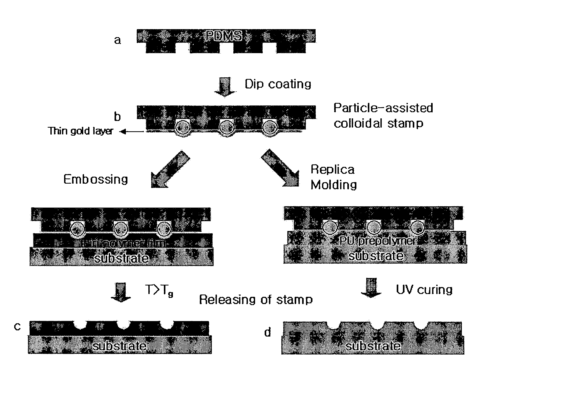
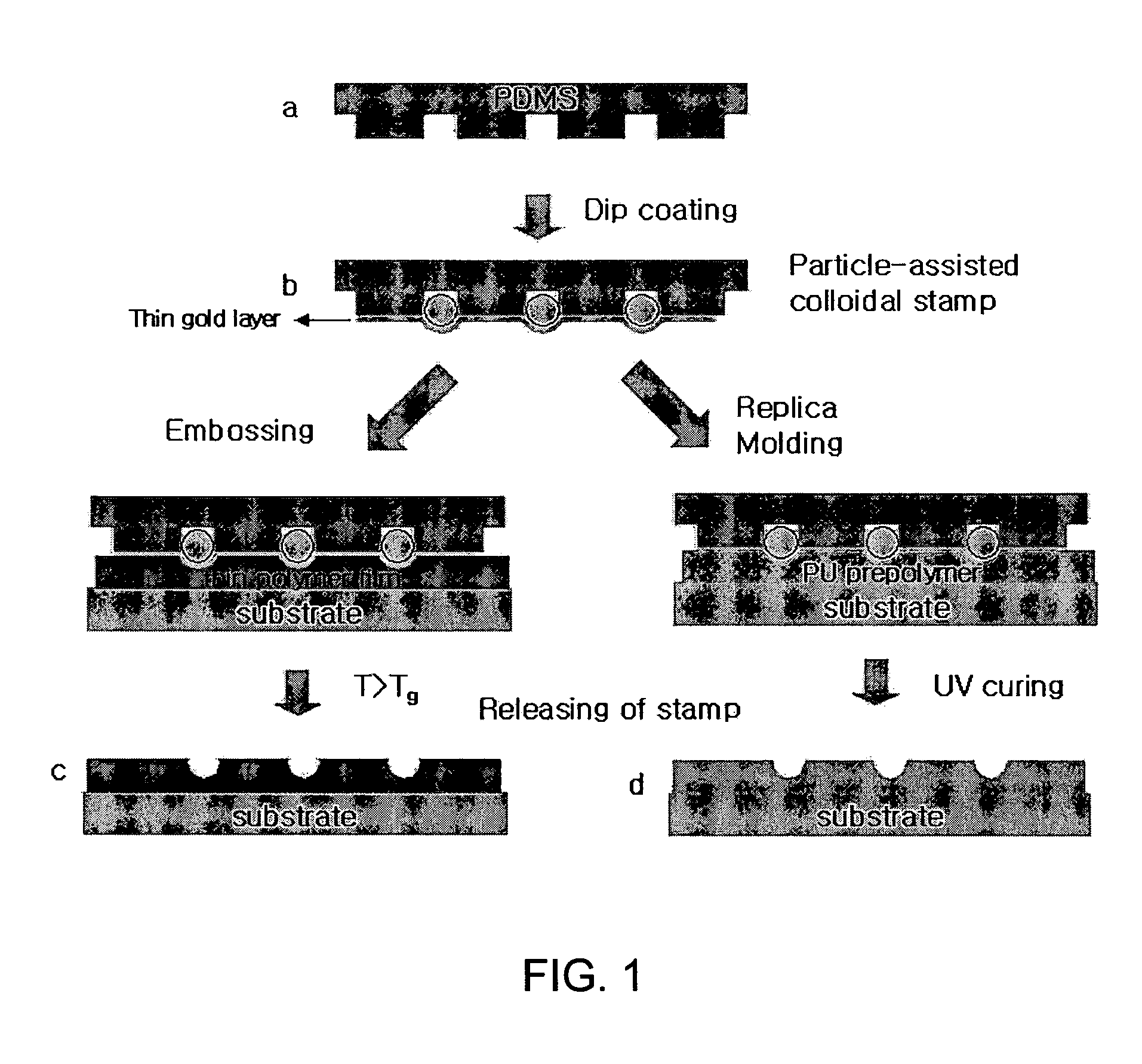
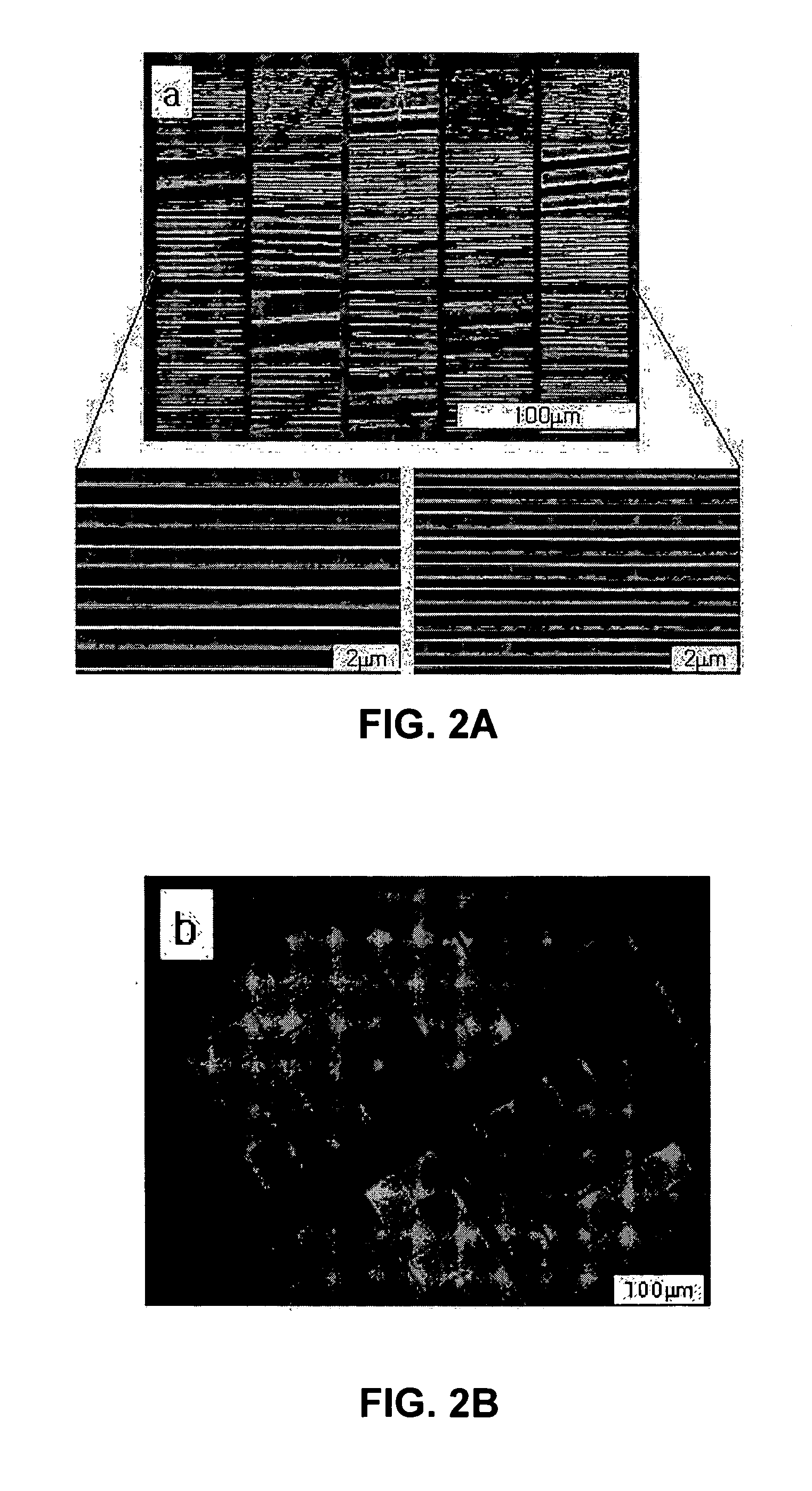
[0055]To fabricate a soft polymer mold having line widths of various sizes, a quartz master produced by electron beam lithography process was used. First, polydimethylsiloxane (PDMS) as a soft polymer material was poured on the master and then cured at 80° C. for 1 hour. FIG. 2A is an electron micrograph of the PDMS mold, which was poured to the master, replicated and then completely cured. FIG. 2B is an optical micrograph of the same PDMS mold, which displays different colors (in this figure, as shades of gray) by being scattered by various line widths.

[0056]Thereafter, particles were filled into the patterned soft polymer mold through a dip coating process. As such, the particles included spherical silica particles having a uniform size of 300 nm. The dip coating process was performed at 200 nm / sec. Further, since the dip coating was determined by surface tension and speed, the above parameters should be optimized fo...

example 2

Preparation of Complex Pattern of Polymer and Particles by Replica Molding

[0059]Example 2 was prepared similar to Example 1, with the exception that the gold film was not coated on the stamp. In cases where the stamp was not coated (with the gold film serving to prevent the impregnation of the polymer precursor into the stamp), all the particles were separated from the stamp and buried in the polyurethane polymer film. Therefore, as shown in FIGS. 5A and 5B, a complex pattern of embossed silica particles and polymer results resulted, instead of the engraved polymer pattern.

example 3

Preparation of Polymer Pattern by Nano-imprinting (Embossing)

[0060]Before the nano-imprinting process, about 1 μm sized polystyrene film was spin-coated onto a silicon wafer and then dried. On the polystyrene coating layer, the gold film-coated stamp shown in FIGS. 3A to 3F was placed and allowed to stand at temperatures higher than a glass transfer temperature of 110° C., at which the polystyrene began to flow. After a predetermined time, the stamp was released, and the engraved porous polystyrene patterns shown in FIGS. 6A to 6D were obtained.

[0061]As described hereinbefore, the present invention provides a method of fabricating a patterned polymer film on a nanometer scale. This is advantageous in that polymer patterns having nanometer sized line widths therebetween, which are difficult to realize by a photolithography or electron beam process, can be quickly and inexpensively fabricated at desired positions by use of a self-assembling process and a soft lithography process.


PUM


Abstract

A method of fabricating a patterned polymer film with nanometer scale includes filling particles each having a predetermined size in a pattern provided to a soft polymer mold to prepare an embossed stamp; placing the embossed stamp on a desired polymer film; allowing the embossed stamp placed on the polymer film to stand at temperatures higher than a glass transfer temperature of the polymer film for a predetermined time; and releasing the embossed stamp from the polymer film. Alternatively, the patterned polymer film is obtained by filling particles each having a predetermined size in a pattern provided to a soft polymer mold to prepare an embossed stamp; placing the embossed stamp on a coating layer of a polymer precursor formed on a substrate; curing the coating layer; and releasing the embossed stamp from the cured coating layer.

Description

[0001]This application claims priority to Korean Patent Application No. 2003-42676, filed Jun. 27, 2003, which is incorporated herein by reference in its entirety.BACKGROUND OF THE INVENTION[0002]1. Field of the Invention[0003]The present invention relates to preparation methods of regular polymer patterns for the fabrication of small electronic and optical devices, and methods of fabricating a nano-patterned polymer film, characterized in that polymer patterns having nanometer sized line widths therebetween (which are difficult to realize by a photolithography or electron beam process) can be quickly and inexpensively fabricated at desired positions by use of a self-assembling process and a soft lithography process.[0004]2. Related Art[0005]Research on new fabrication processes for fine patterns having 100 nanometer or less scale, instead of a conventional photolithography process, has been a subject of much interest recently. Miniaturization and high integration of semiconductor d...

Claims


Application Information

Patent Timeline
IPC IPC(8): B05D5/12H01L21/027B05D1/42G03F7/00H01L51/40
CPCB05D1/42B82Y10/00G03F7/0002B82Y40/00H01L51/0004H10K71/13H01L21/027
Inventor YANG, SEUNG-MANJANG, SE GYUCHOI, DAE-GEUN
Owner KOREA ADVANCED INST OF SCI & TECH
Learn More