Manufacturing process for annealed wafer and annealed wafer
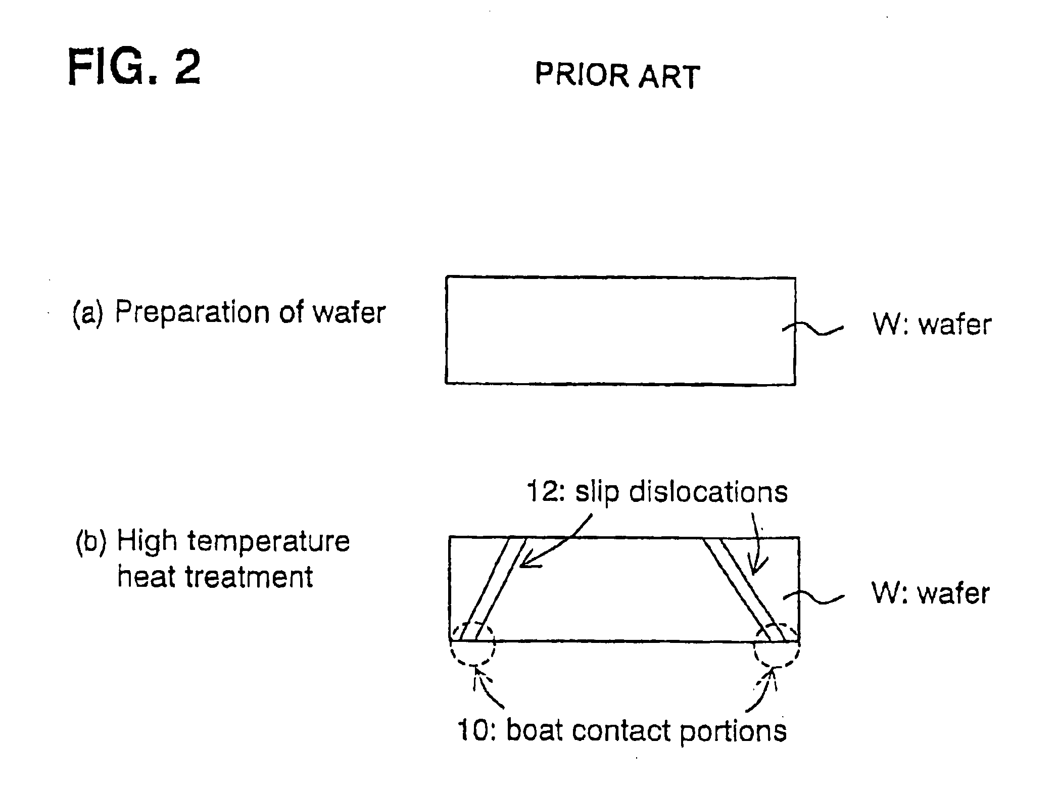
a technology of annealing wafers and manufacturing processes, which is applied in the direction of crystal growth processes, polycrystalline material growth, and under a protective fluid, can solve the problems of large slip dislocations (long slip dislocations in length) that are generated remarkably, and cannot avoid these slip dislocations by modifying the shape of the boat, so as to achieve the effect of reducing the ra
- Summary
- Abstract
- Description
- Claims
- Application Information
AI Technical Summary
Benefits of technology
Problems solved by technology
Method used
Image
Examples
example 1
[0034]A diameter of 300 mm, p type, a crystal axis orientation , a resistivity of 10 Ωcm, a nitrogen concentration of 5×10¹³ atoms / cm3, and an initial interstitial oxygen concentration of 14 ppma (values as measured in accordance with Japan Electronic Industry Development Association (JAIDA) standard)
[0035]800° C., 4 hr+1000° C., 16 hr; a 100% argon atmosphere
[0036]1200° C., 1 hr; a 100% argon atmosphere
[0037]1) Observation of slip dislocations is performed by the X-ray topographic method.
[0038]2) A DZ layer and an oxide precipitate density are measured by observation under an optical microscope of a wafer etched with a preferential etching solution containing no hexa-valent chromium ion according to a testing method of crystal defects in silicon by preferential etching method priscribed in Japanese Industrial Standard (JIS H 0609:1999) after angle polishing.
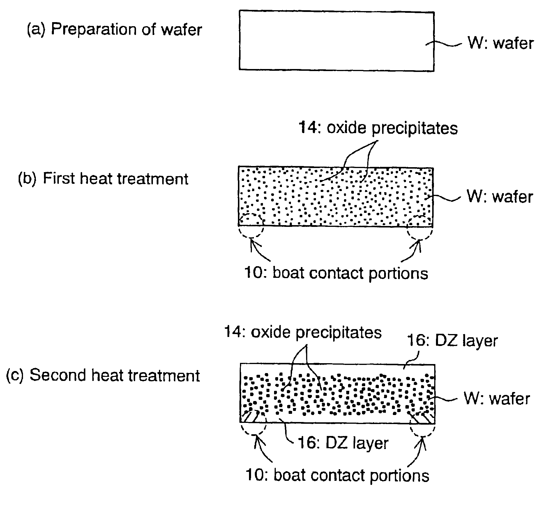
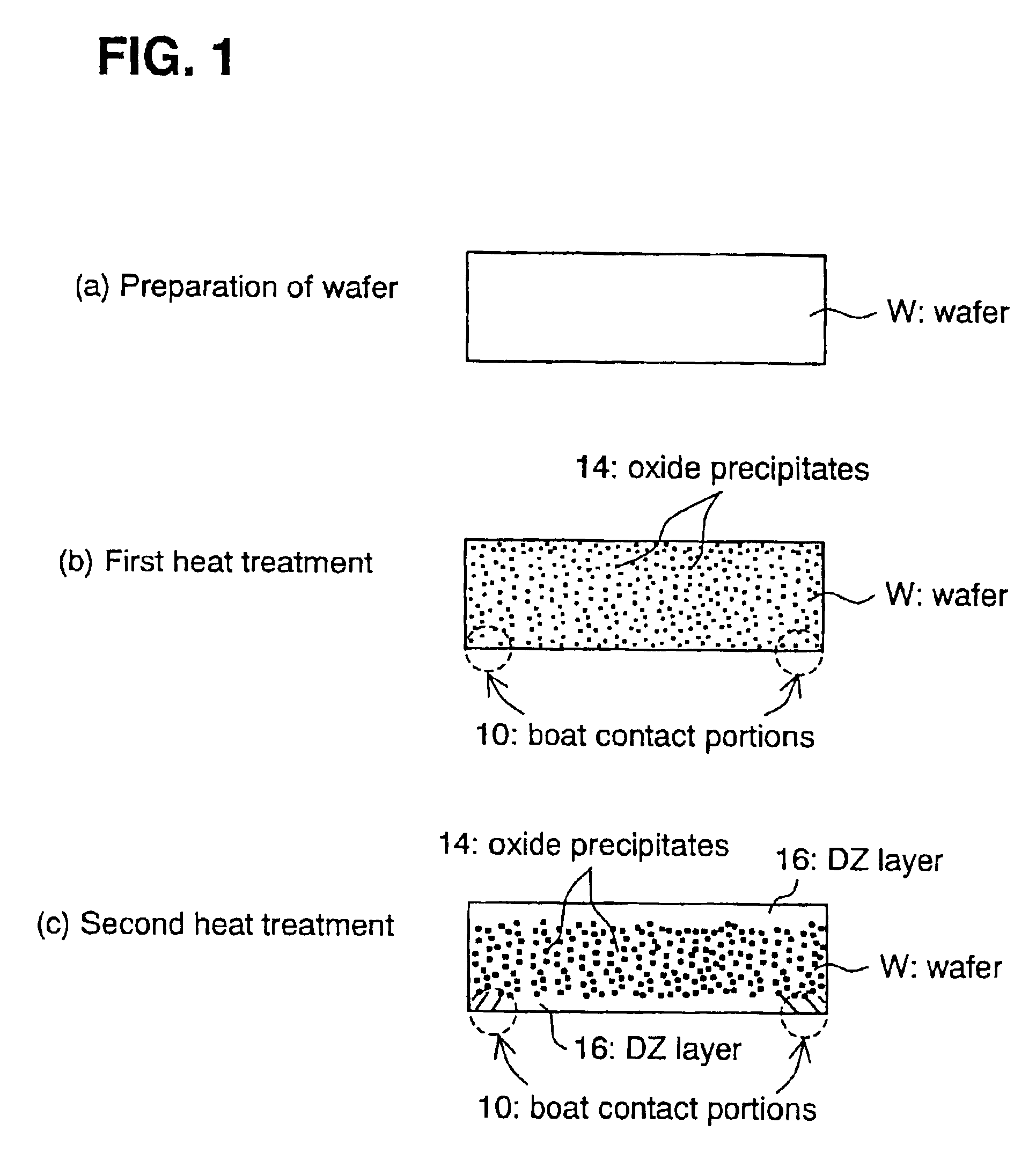
[0039]The wafer above described was subjected to the first heat treatment and the second heat treatment under the above-mentio...
example 2
[0041]A diameter of 300 mm, p type, a crystal axis orientation , a resistivity of 10 Ωcm, undoped with nitrogen, and an initial interstitial oxygen concentration of 16 ppma
[0042]700° C., 4 hr+1000° C., 8 hr; a nitrogen atmosphere with an oxygen concentration of 3%
[0043]1150° C., 4 hr; a 100% argon atmosphere
[0044]The first heat treatment and the second heat treatment were applied to the wafer under the above-mentioned conditions, then slip dislocations, a DZ layer and an oxide precipitate density were measured in a similar way as in Example 1, and results of the measurements are shown in Table 1. As shown in Table 1, in Example 2, no generation of slip dislocations in the wafer was observed, a DZ layer with a sufficient width was formed in a surface layer section thereof and an oxide precipitate density in the bulk thereof was sufficiently high.
PUM
| Property | Measurement | Unit |
|---|---|---|
| temperature | aaaaa | aaaaa |
| temperature | aaaaa | aaaaa |
| temperature | aaaaa | aaaaa |
Abstract
Description
Claims
Application Information


