Method of observation by transmission electron microscopy

ransmission electron technology, applied in the direction of individual semiconductor device testing, semiconductor/solid-state device testing/measurement, instruments, etc., can solve the problems of affecting the observation of defects or the like in the metallic section, affecting the distribution condition of defects in amorphous materials, and affecting the withstand voltage of device elements. , to achieve the effect of improving the withstand voltage reducing the sensitivity of the device element, and improving the sensitivity of the a transmission electron microscopy observation method of transmission electron microscopy observation method, transmission electron microscopy and transmission electron microscopy and transmission electron micro transmission electron microscopy and transmission electron microscopy, which is applied in the field which is applied in the field of transmission electron microscopy transmission field

Inactive Publication Date: 2006-08-01
NISSAN ARC +1
View PDF6 Cites 2 Cited by
  • Summary
  • Abstract
  • Description
  • Claims
  • Application Information

AI Technical Summary

Benefits of technology

[0012]According to an aspect of the invention, there is provided a method for observing defect in an amorphous material by transmission electron microscopy, comprising the steps of: incident electron beam into the amorphous material; eliminating a generated diffraction wave to form an image only by a transmission wave coming through the amorphous material; and observing the image under an under-focus condition.

Problems solved by technology

Through the process of development of various materials and of devices, grasping the distribution condition of defects in an amorphous material is a critical issue.
For instance, when pores penetrate the insulating film to create continued pores, they form what is called the “leak path” , which induces leak current and degradation in withstand voltage of the device element.
Accordingly, observation of defects or the like in the metallic sections often becomes inadequate under the same observation condition with that for the amorphous insulating layer.

Method used


Image

  • Method of observation by transmission electron microscopy
  • Method of observation by transmission electron microscopy
  • Method of observation by transmission electron microscopy

Examples


examples

[0072]The embodiment of the invention will be described in more detail referring to the examples.

first example

[0073]The TEM observation has been given to the respective materials for porous interlayer insulating films: a siloxane resin having the main structure of Si—O bond; a fluorine-laid silicon oxide (SiOF); and an organic polymer resin having an aromatic hydrocarbon structure.

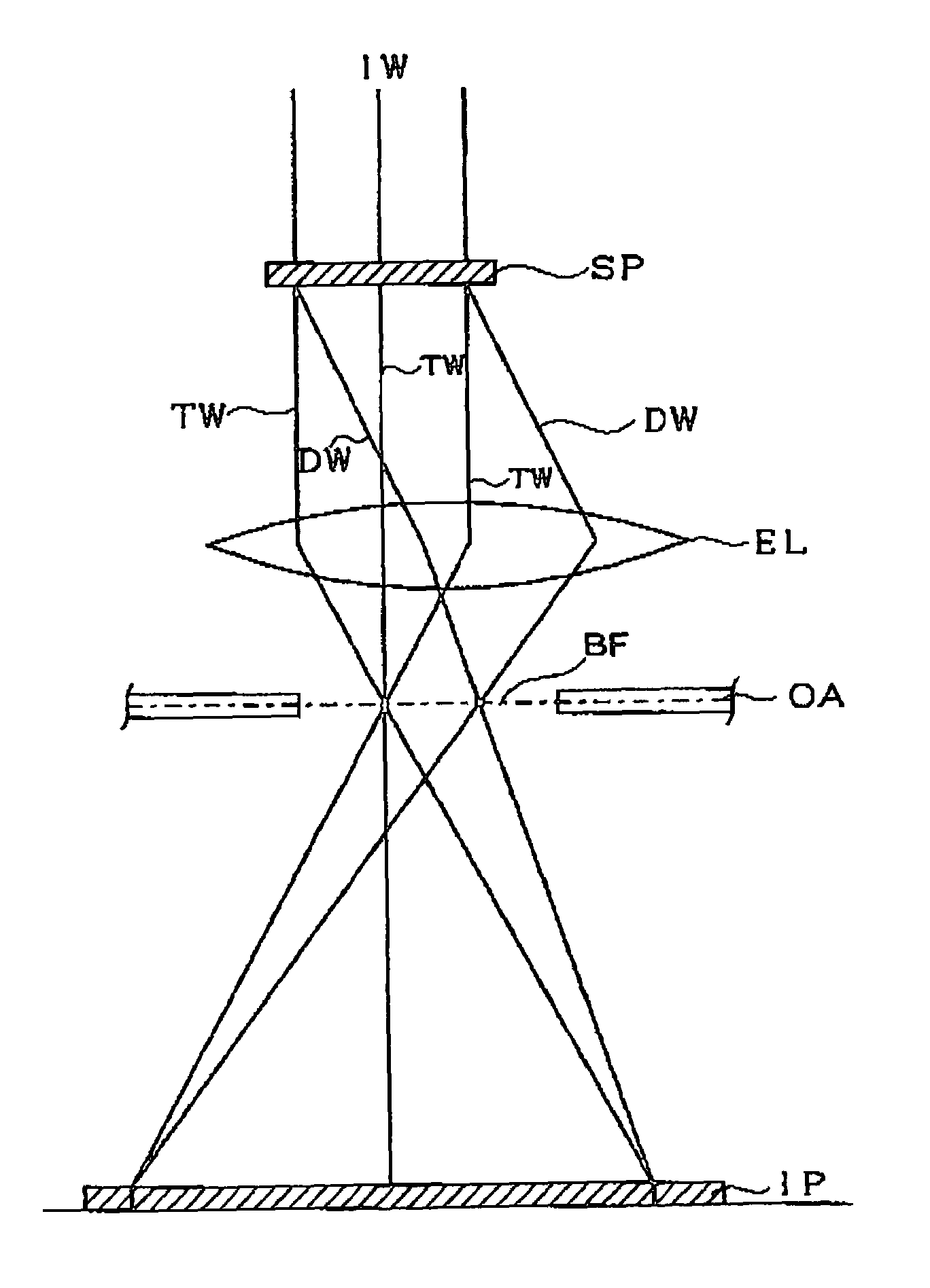
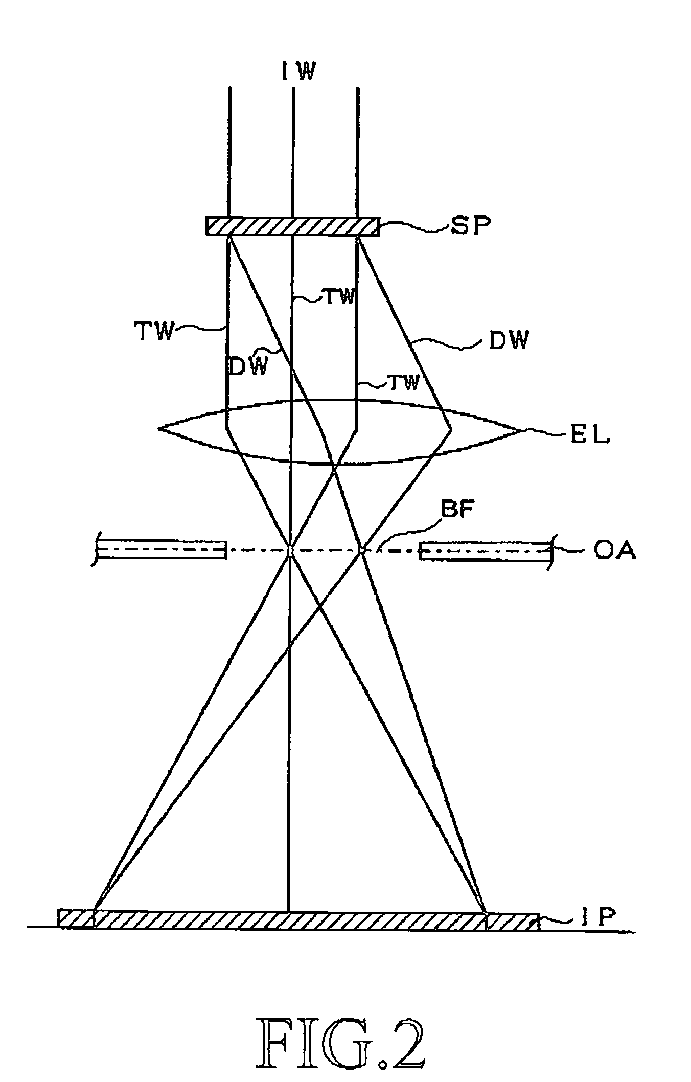
[0074]The specimen for the TEM observation has been sliced to a wedge shape, and thinned to 200 nm or smaller thickness using focused ion beam (FIB). To prevent charge-up of the insulating film, the specimen may be coated by carbon (C) to thickness from several nanometers to several tens of nanometers. Nevertheless, an experiment conducted by the inventors of the present invention has shown that the insulating film which has been thinned to the above-described thickness range has not substantially shown deformation of the TEM image caused by the charge-up even without that kind of conductive coating, and that the observation has been conducted without problem.

[0075]When conducting the TEM observation, the size of ...

second example

[0079]As the Second example of the embodiment of the invention, observation has been given on a composite material having an amorphous material and a crystalline material.

[0080]FIG. 12 is a typical drawing of the cross sectional structure of a semiconductor integrated circuit device, observed in the Second example. The semiconductor device is a logic type device, and has a multilayer interconnection structure.

[0081]In the case of the semiconductor device, an N-well 12 and a P-well 13 are respectively formed on the surface of a silicon substrate 11, and a MOS transistor is formed on the respective surface layers thereof. The upper face of the transistor is covered with a first interlayer insulating film 20. Each of source, drain, and gate 14 of the transistor is provided with a silicide 15 as the electrode contact. The silicide 15 is connected with a first metallic interconnection layer 22 above thereof via a contact hole opened in the first interlayer insulating film 20 and via a bu...


PUM

PropertyMeasurementUnit
tilted anglesaaaaaaaaaa
thicknessaaaaaaaaaa
tilt angleaaaaaaaaaa

Abstract

A method for observing defects in an amorphous material by transmission electron microscopy. The method generates an incident electron beam into the amorphous material, eliminates a generated diffraction wave to form an image only by a transmission wave coming through the amorphous material, and observes the image under an under-focus condition.

Description

BACKGROUND OF THE INVENTION[0001]1. Field of the Invention[0002]The present invention relates to a method of observation by the transmission electron microscopy, and particularly to an observation method by the transmission electron microscopy capable of clearly observing the distribution condition of defects such as pores in an amorphous material.[0003]1. Discussion of the Background[0004]Through the process of development of various materials and of devices, grasping the distribution condition of defects in an amorphous material is a critical issue. In the development of semiconductor integrated circuit devices, for example, the interconnection rule has entered a generation of 100 nanometer level, thus the higher integration requires a multilayer interconnection structure applying an interconnection layer made of copper and an interlayer insulating layer made of an insulating material.[0005]In a semiconductor device having that type of multilayer interconnection structure, the die...

Claims


Application Information

Patent Timeline
Patent Type & Authority Patents(United States)
IPC IPC(8): H01L21/66H01L21/00G01N23/04H01J37/21H01J37/26
CPCG01N23/04H01J2237/262H01J2237/2611G01N2223/102G01N23/041
Inventor OGAWA, SHINICHIINOUE, YASUHIDESHIMANUKI, JUNICHIMORI, HIROTARO
Owner NISSAN ARC
Why Eureka
Try Eureka