
Scanning kelvin microprobe system and process for analyzing a surface

Inactive Publication Date: 2006-08-01
SENSORCHEM INT
View PDF11 Cites 24 Cited by
  • Summary
  • Abstract
  • Description
  • Claims
  • Application Information

AI Technical Summary

Benefits of technology

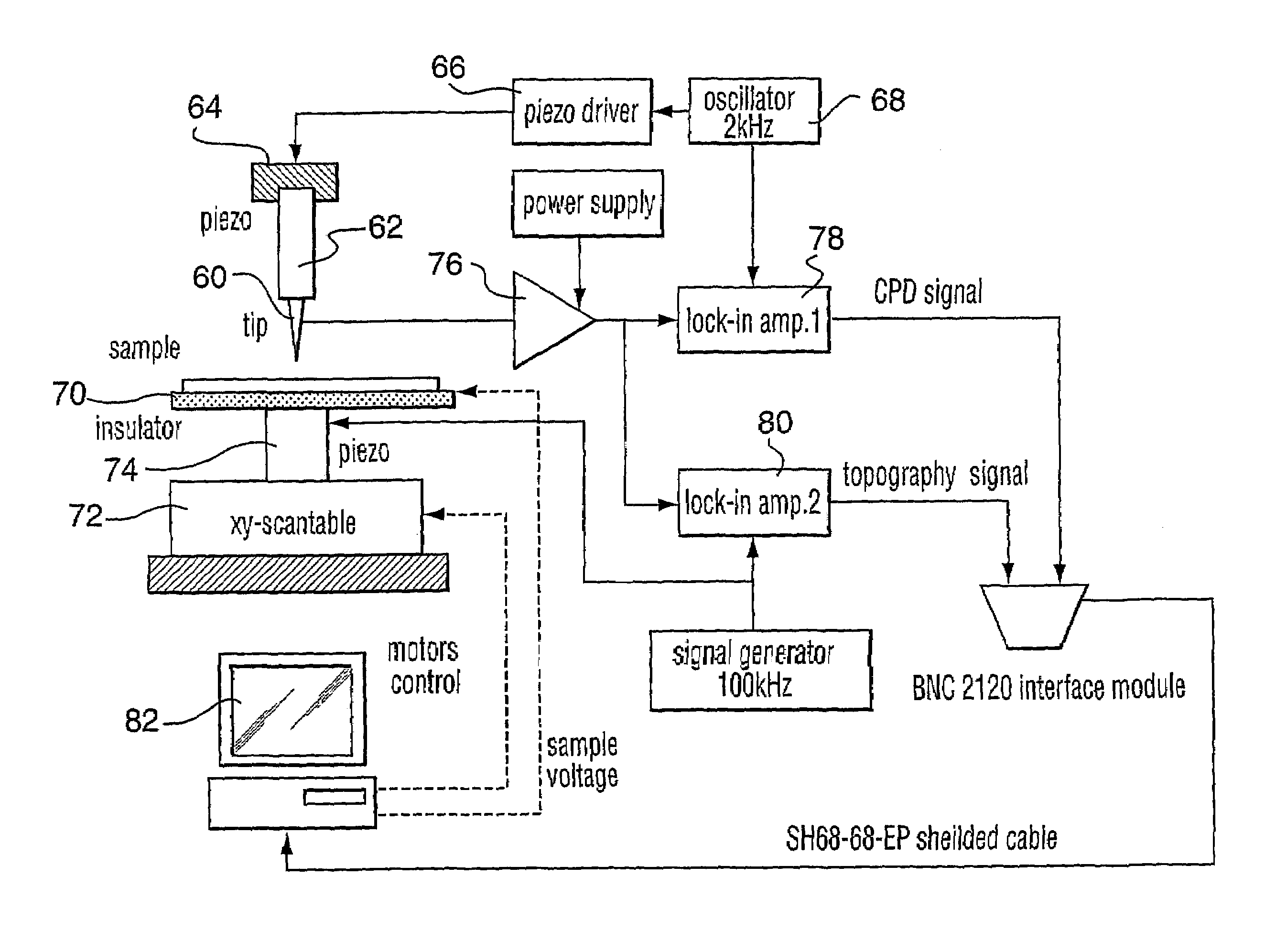
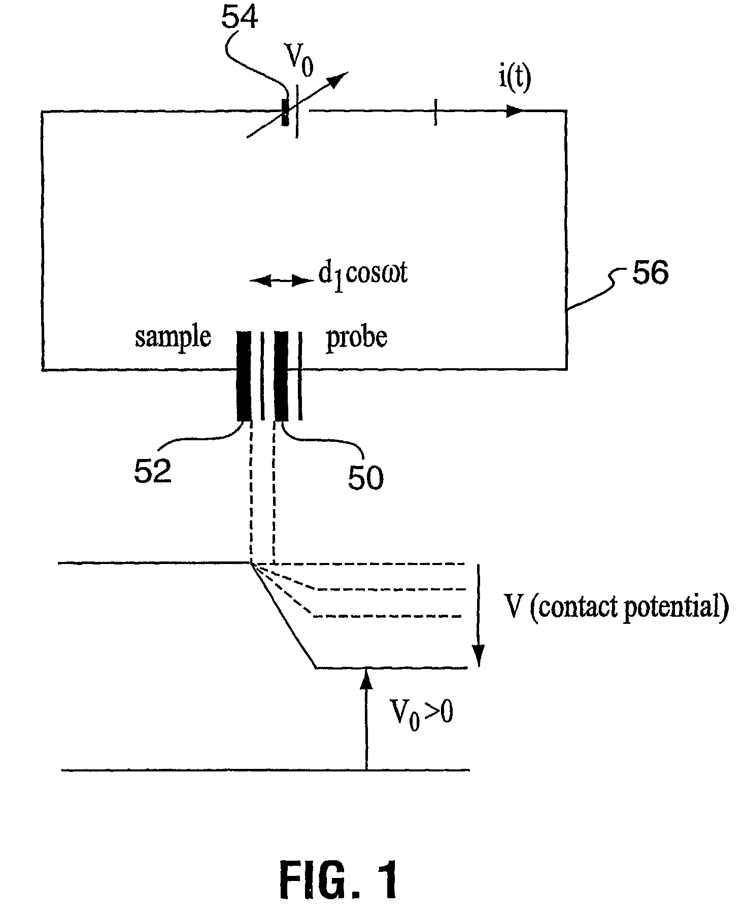
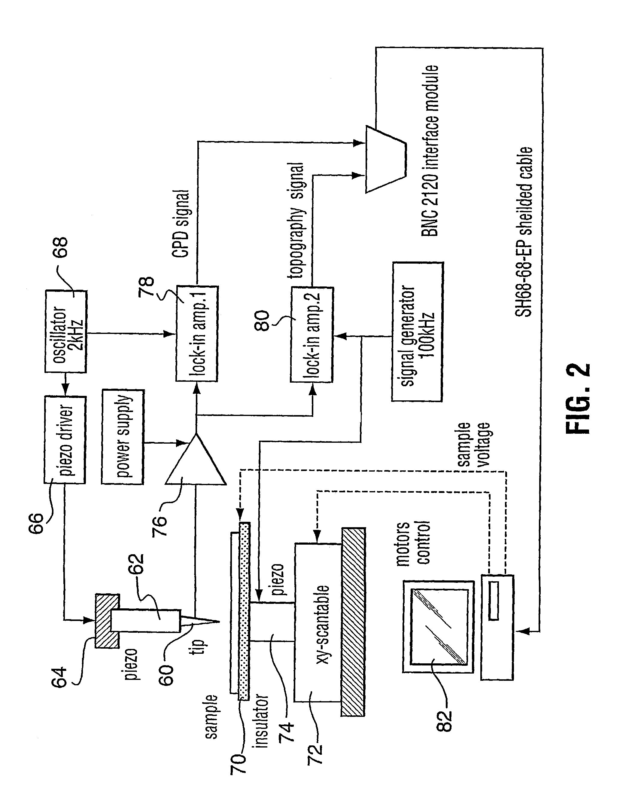
[0012]The SKM system of the invention uses a higher frequency (sample-tip capacitance detection) to control the sample-tip distance, thus, making the process stable and reliable. The automated monitoring of the contact potential and topography was achieved using 2 lock-in amplifiers tuned respectively on the vibrational frequency and on the capacitance-detection frequency. This means that the monitoring of the sample-tip distance is no longer achieved by processing the harmonics of the CPD signal as taught by the prior art, but by measuring the sample-tip capacitance at a frequency above the vibrational frequency. This approach solves the instability and unreliability problems that affect the prior art. The current prototype has a superior lateral resolution achieved by employing amplifiers capable of detecting low-level currents extracted by extremely fine tip probes having an apex radius of curvature below 100 nm. The invention advantageously comprises a data acquisition and imagining system. Further, the null-condition measurement according to the invention avoids the strong electric fields that affect the surface of the specimens in prior art apparatuses. This is also an advantage over the force microscopes operating in Kelvin mode that develop extremely high local electrical fields (109 V / m range), thus affecting both the local distribution of charges and the spatial conformation of the investigated molecules.

Problems solved by technology

This means that the monitoring of the sample-tip distance is no longer achieved by processing the harmonics of the CPD signal as taught by the prior art, but by measuring the sample-tip capacitance at a frequency above the vibrational frequency.

Method used


Image

  • Scanning kelvin microprobe system and process for analyzing a surface
  • Scanning kelvin microprobe system and process for analyzing a surface
  • Scanning kelvin microprobe system and process for analyzing a surface

Examples


example 1

Characterizing Metals

[0079]A number of metallic surfaces including Pt, Au, Ag, Sn, Pb and Al are examined. Patterned surfaces are obtained by sputtering of Pt layers on Ag and Si, Au layers on Pd and Ag, and metals on silicon and mica substrates.

[0080]FIG. 4 illustrates a CPD image obtained from a silver surface. FIG. 5 is a CPD image of a silver surface after surface treatment. FIG. 6 is a CPD image of silver on a mica surface. FIG. 7 illustrates the topography of silver on a mica surface.

example 2

Characterizing Conductors

[0081]Highly ordered-pyrolitic graphite samples are analyzed. FIG. 8 illustrates the topography of a graphite surface. FIG. 9 is a CPD image of a highly-ordered pyrolitic graphite surface.

example 3

Microelectronic Fabrication

[0082]FIGS. 10A and 10B show a measure of the capabilities of the instrument by providing a tandem measurement of topography and CPD. FIG. 10A depicts a topographical image of the edge presented by a layer of aluminum deposited on a silicon wafer in a typical microelectronic fabrication process. The edge is supposed to be vertical with a steep height of about 1 μm. This particular topographical image was realised at a spatial resolution of 2 μm. Note that the second axis represents (in V) the displacement of the piezoelectric table and for 1V the piezoelectric material expands 20 μm. Accordingly, the aluminum layer appears to have a surface height variation of about 400 nm (0.02V). Secondly, it can be seen that the edge actually slopes over 20 μm (x-axis). FIG. 10B shows a tandem CPD image. Note that the image is both rotated at 90° and inverted in order to highlight the difference in contact potential between aluminum and silicon (the flat, bottom surface...


PUM


Abstract

A scanning Kelvin microprobe (SKM) system capable of measuring and analyzing surface characteristics of samples is provided. Also provided is a process of measuring and analyzing surface characteristics of samples. Further, there are provided uses of the SKM system in measuring and analyzing surface characteristics of conductors, semiconductors, insulators, chemicals, biochemicals, photochemicals, chemical sensors, biosensors, biochemical microarrays, microelectronic devices, electronic imaged devices, micromachined devices, nano-devices, corroded materials, stressed materials, coatings, adsorbed materials, contaminated materials, oxides, thin films, and self assembling monolayers.

Description

[0001]This application is a 371 of international application PCT / CA01 / 00717 filed on May 18, 2001.FIELD OF THE INVENTION[0002]This invention relates to processes for measurement and analysis of surfaces utilizing Kelvin methodology, and more specifically to the development and use of an improved scanning Kelvin microprobe (SKM) for surface measurement and analysis.BACKGROUND OF THE INVENTION[0003]The Kelvin method for the measurement of work function can be employed for the analysis of a wider range of materials, at different temperatures and pressures, than any other surface analysis technique. Work function is a very sensitive parameter which can reflect imperceptible structural variations, surface modification, contamination or surface-related processes. The method is now regaining popularity1-4 as a powerful technique because of its inherent high surface sensitivity, high lateral resolution due to the availability of nanometric precision-positioning systems, and improved signal ...

Claims


Application Information

Patent Timeline
IPC IPC(8): G01R31/26G01N27/00G01N33/543G01Q10/00G01Q10/04G01Q10/06G01Q60/30
CPCB82Y35/00G01Q60/30G01N33/5438G01N27/002
Inventor THOMPSON, MICHAELCHERAN, LARISA-EMILIA
Owner SENSORCHEM INT
Learn More