High power semiconductor laser with a large optical superlattice waveguide
a superlattice waveguide and semiconductor laser technology, applied in lasers, laser cooling arrangements, laser details, etc., can solve the problem of difficult to achieve good composition control, achieve low vertical farfield, reduce optical losses, and reduce optical loss
- Summary
- Abstract
- Description
- Claims
- Application Information
AI Technical Summary
Benefits of technology
Problems solved by technology
Method used
Image
Examples
Embodiment Construction
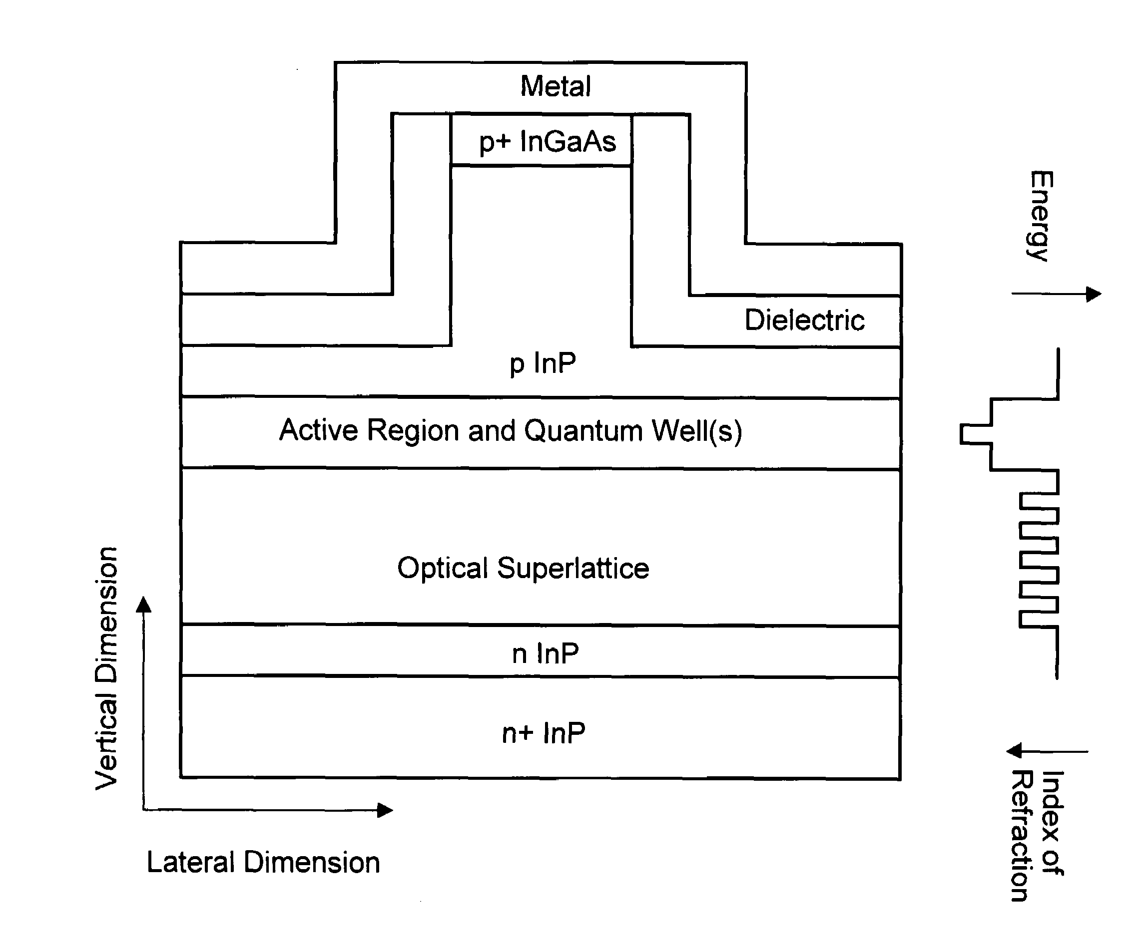
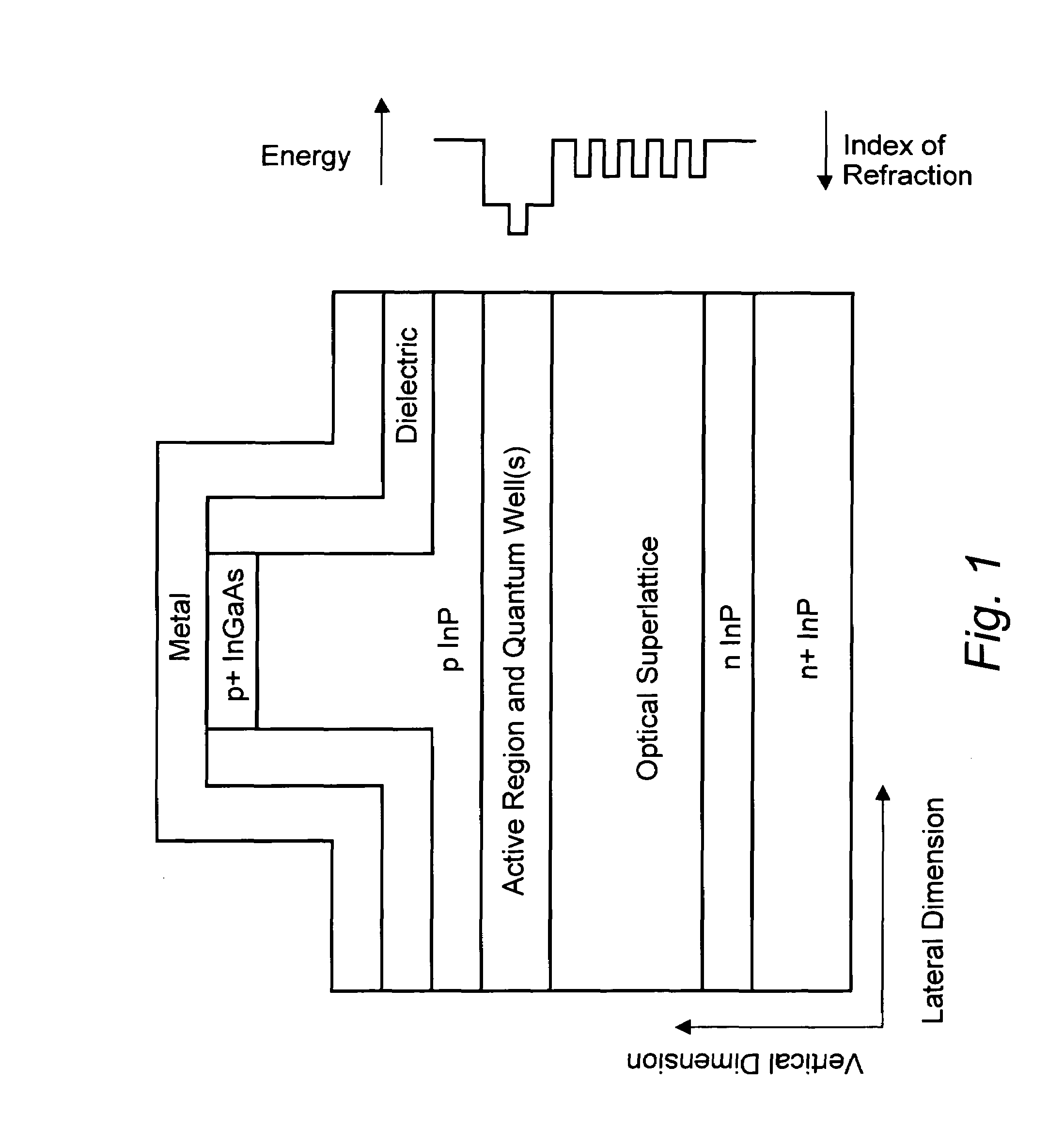
[0035]FIG. 1 shows the basic layout, i.e. the cross section of the essential parts, of a semiconductor laser diode according to the invention, together with the distribution of the associated refraction index on the right. Starting from the bottom of the structure shown in FIG. 1, the n+InP layer represents the InP substrate for the epitaxial growth of the laser structure, followed by an n InP layer, both known from the prior art. On this lower cladding layer, the optical superlattice is located, followed by the laser's active region with a gain region and a waveguide. Preferably the optical superlattice terminates towards the active region with a material with low index of refraction and therefor high bandgap. Most preferably the material with low index of refraction consists of InP. On top of the active region, another cladding layer, here of p InP is situated, forming the laser ridge with a narrow p+InGaAs layer on top of the ridge. The whole structure carries a metallization on ...
PUM
 Abstract
Description
Claims
Application Information


