[0013]In view of the foregoing, an object of the present invention is providing a
semiconductor device that can shallow the junction depths of extended high-concentration dopant diffused layer and pocket dopant diffused layer and can minimize increase in
junction leakage current and a method for fabricating the device.
[0015]In the inventive
semiconductor device, the pocket dopant diffused layer is formed through
diffusion of a dopant of a second
conductivity type that has a large
mass (e.g.,
indium). A dopant with a large
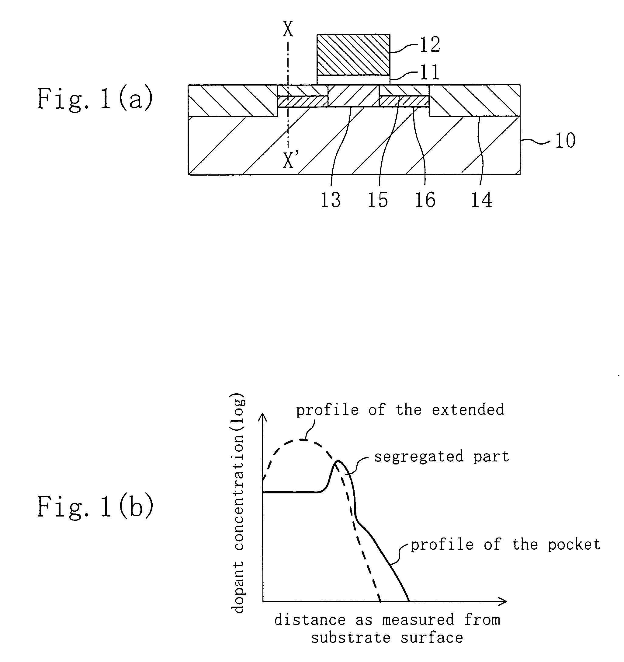
mass shows a small diffusion coefficient in its
thermal equilibrium state. In addition, most of point defects, which have been created in excessive numbers due to the damage involved with implantation, are trapped into a
dislocation loop layer. That is to say, the number of freely movable, diffusible point defects decreases. As a result, the dopant profile of the pocket dopant diffused layer sharpens. Furthermore, the
dislocation loop layer is formed inside the pocket dopant diffused layer and segregated parts are formed in the dislocation loop layer through segregation of the dopant with a large
mass.
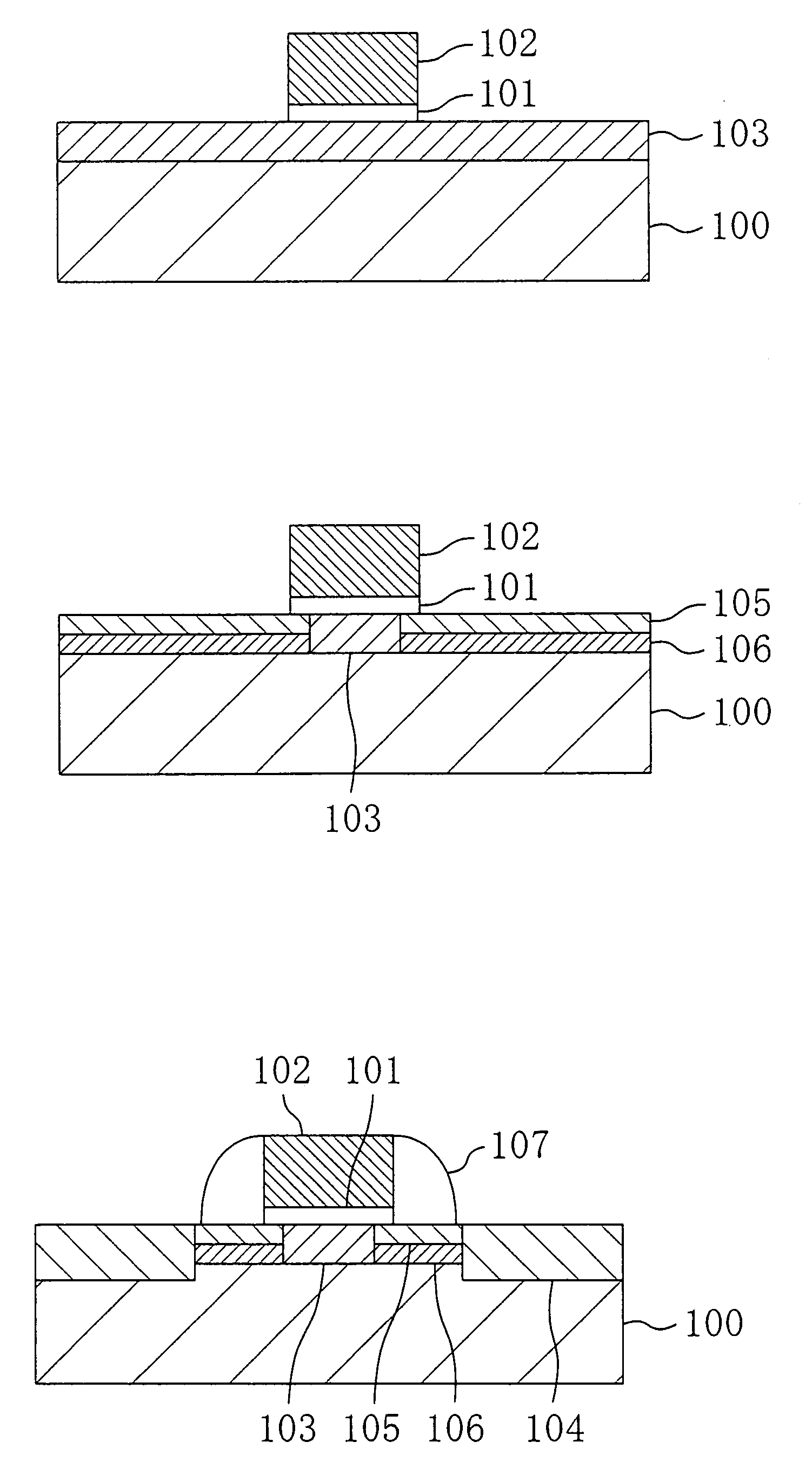
[0016]Accordingly, in the extended high-concentration dopant diffused layer located closer to the surface of the substrate than the pocket dopant diffused layer is, channeling of the first dopant of the first conductivity type is suppressed by an amorphous layer, which has been formed by the dopant of the second conductivity type that has the large mass. Moreover, diffusion of the first dopant is suppressed by the segregated parts of the pocket dopant diffused layer, and therefore the junction will be shallower. As a result, the driving power of the
transistor can be increased and the short channel effects can be minimized, thus greatly contributing to
miniaturization of the transistor.
[0018]According to the inventive method for fabricating a
semiconductor device, after an amorphous layer has been formed in a semiconductor region by implanting heavy ions with a large mass thereto, ions of a first dopant of a first conductivity type are implanted. Thus, channeling of the first dopant is avoidable. Also, a dislocation loop layer is formed near an amorphous / crystalline interface during the annealing process after the ions have been implanted. And
silicon interstitials, which usually cause transient enhanced diffusion, are trapped into the dislocation loop layer. Furthermore, a segregated part is formed in the pocket dopant diffused layer through segregation of the heavy ions. As a result, the diffusion of the first dopant of the first conductivity type is suppressed, and the extended high-concentration dopant layer can have a shallower junction.
[0019]According to the semiconductor device and its fabrication process of the present invention, heavy ions with a large
mass number (e.g.,
indium) are used to form the pocket dopant diffused layer. Thus, pre-amorphization effects are attainable by the implantation of the heavy ions. And the dislocation loop layer can advantageously trap the
silicon interstitials. In addition, since
indium is easily trapped and segregated in the dislocation loop layer, the extended high-concentration dopant diffused layer and pocket dopant diffused layer can both have their junctions shallowed and sharpened. Accordingly, a miniaturized semiconductor device and a fabrication process thereof can be provided with the inverse channel effects suppressed.
[0020]Furthermore, in the inventive method for fabricating a semiconductor device, indium ions are implanted at a low energy and at a high
dose to form the pocket dopant diffused layer. In this manner, the profile of the pocket dopant diffused layer can be defined at an optimum level and the dislocation loop layer can be defined not to overlap with a depletion layer in source / drain regions. As a result, the leakage current can be reduced.

