Electron beam apparatus and method of manufacturing semiconductor device using the apparatus

a technology of electromagnetic apparatus and semiconductor device, which is applied in the direction of material analysis using wave/particle radiation, instruments, nuclear engineering, etc., can solve the problems of a long testing time, inferior throughput of electromagnetic beam based defect testing apparatus, etc., and achieve the effect of improving the throughput of inspection processing

Active Publication Date: 2006-08-22
EBARA CORP
View PDF16 Cites 45 Cited by
  • Summary
  • Abstract
  • Description
  • Claims
  • Application Information

AI Technical Summary

Benefits of technology

[0009]The present invention has been accomplished with a view to obviating the aforementioned problems of prior art and therefore, it is an object of the present invention to provide an evaluation system employing an SEM electron beam apparatus of a multi-beam type and especially an evaluation system capable of improving a throughput of inspection processing.
[0010]It is another object of the present invention to provide an SEM electron beam apparatus of a multi-beam type capable of improving not only a throughput of inspection processing but also detection accuracy.

Problems solved by technology

However, the electron beam based defect testing apparatus also has a disadvantage in that it is inferior to the optical one in the throughput.
However, it takes so long testing time that it is expected to develop a defect testing apparatus which can rapidly conduct a test.
Further, a testing apparatus is expensive and low in throughput as compared with other process apparatuses, so that it is presently used after critical steps, such as after etching, deposition (including copper coating), CMP (chemical-mechanical polishing) planarization processing, and so on.
Therefore, there exists a problem that a testing speed is significantly low in comparison with that in an optical based testing apparatus.
If a beam current is increased in order to achieve a high throughput, a satisfactory SEM image cannot be obtained in the case of a wafer having an insulating membrane on its surface because charging occurs.
Further, a shadow occasionally appears on an image and secondary electrons from a plurality of electron beams are difficult to separate from one another, which disadvantageously results in a mix of the secondary electrons.
Still further, there has been no suggestion or consideration about an interaction between an electron beam apparatus and other sub-systems in an evaluation system employing a multi-beam based electron beam apparatus and thus, at present there aren't any complete evaluation systems of a high throughput.

Method used


Image

  • Electron beam apparatus and method of manufacturing semiconductor device using the apparatus
  • Electron beam apparatus and method of manufacturing semiconductor device using the apparatus
  • Electron beam apparatus and method of manufacturing semiconductor device using the apparatus

Examples


Embodiment Construction

[0084]In the following, embodiments of a evaluation system according to the present invention will be described in a case that evaluation samples are semiconductor substrates or wafers having patterns on surfaces thereof. It should be noted that samples other than the wafer are applicable.

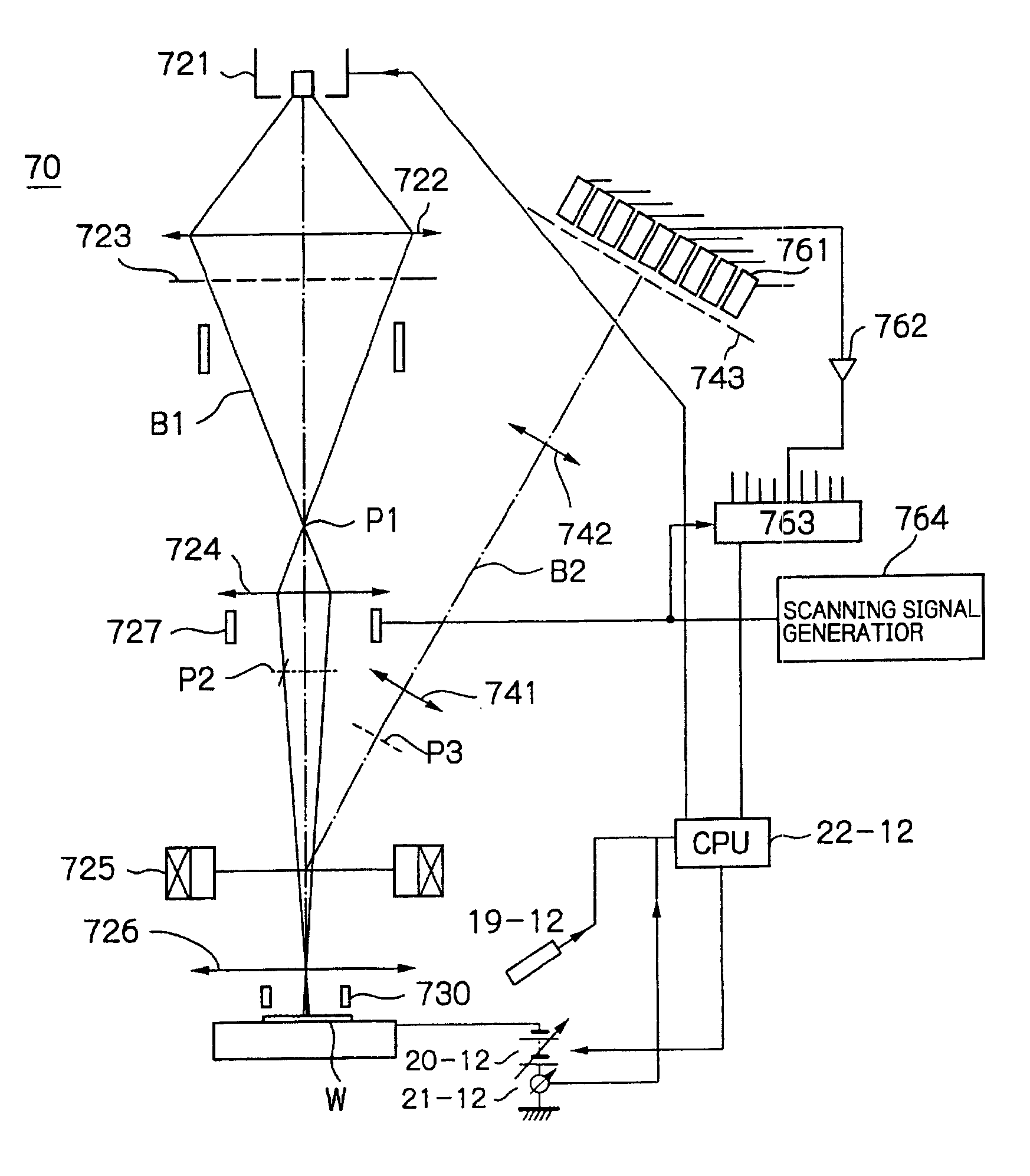
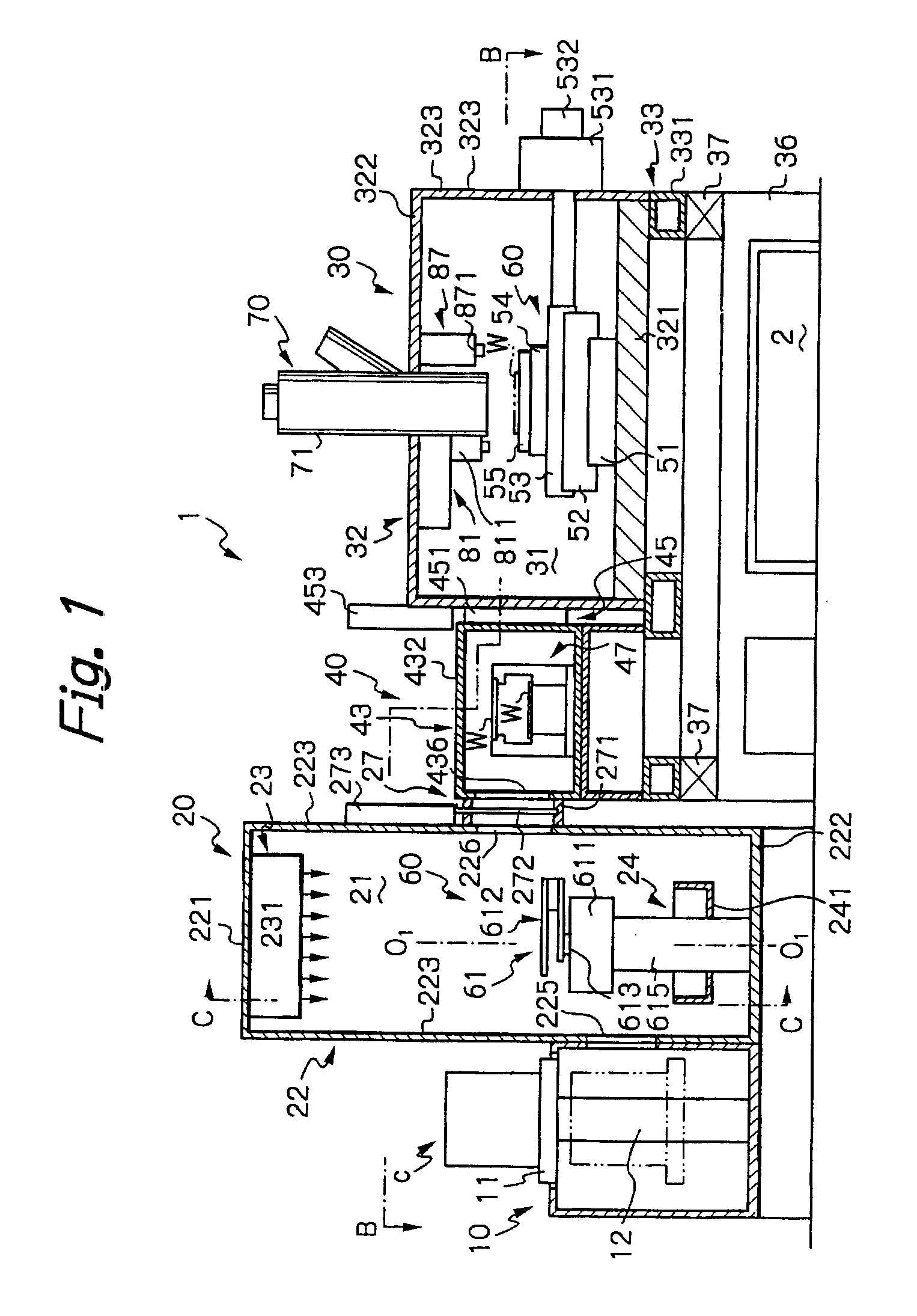
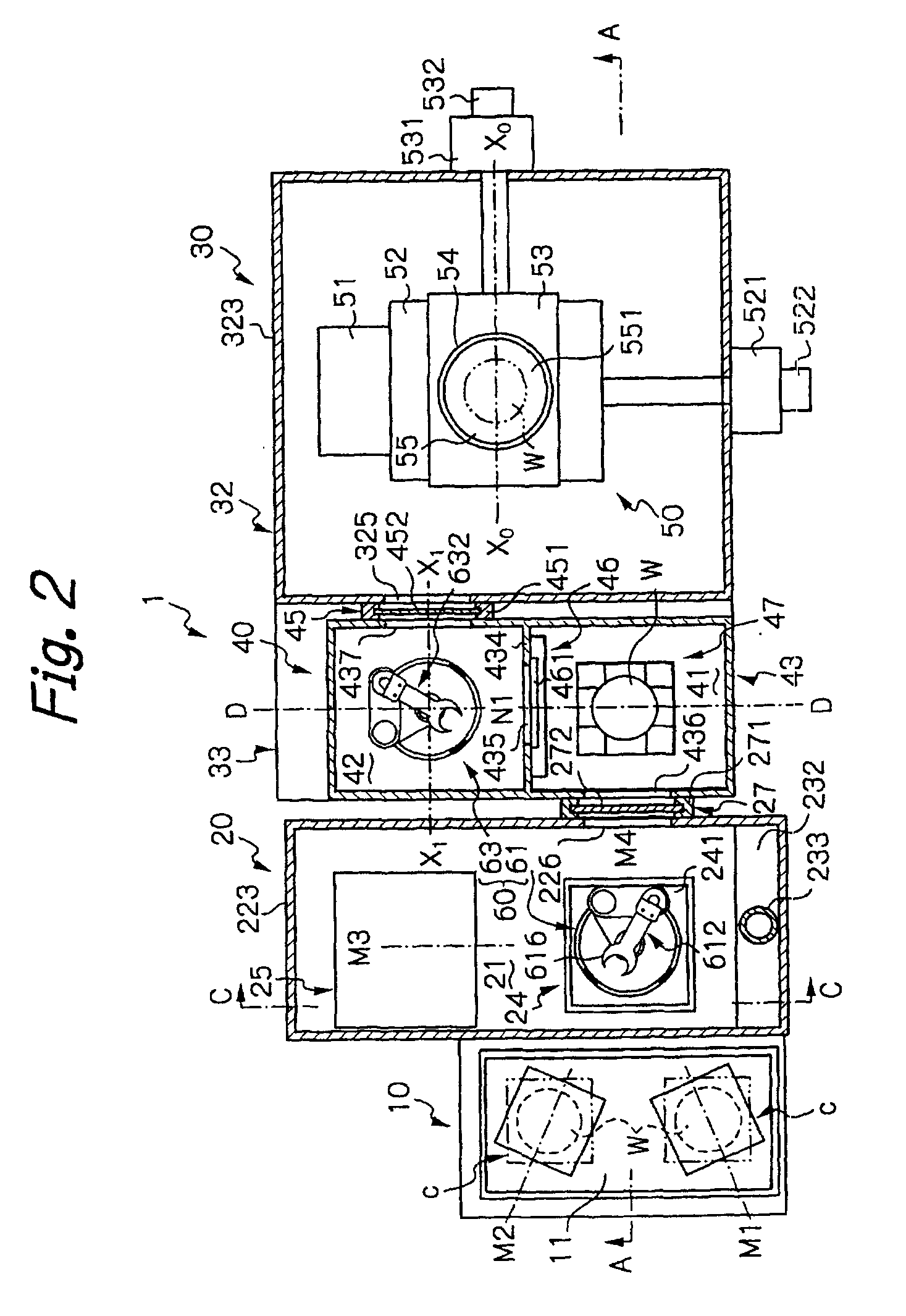
[0085]FIGS. 1 and 2 respectively shows a cross-sectional and plan views illustrating main components of evaluation system 1 according to an embodiment of the present invention. The evaluation system 1 comprises a cassette holder 10 for holding a cassette which stores a plurality of wafers; a mini-environment chamber 20; a main housing 30; a loader housing 40 disposed between the mini-environment chamber 20 and the main housing 30 to define two loading chambers; a loader 60 for loading a wafer from the cassette holder 10 (onto a stage apparatus 50 disposed in the main housing 30); the stage apparatus 50 for carrying and moving the wafer W; and an electro-optical system 70 installed in the vacuum mai...


PUM

PropertyMeasurementUnit
widthaaaaaaaaaa
diameteraaaaaaaaaa
diameteraaaaaaaaaa

Abstract

The present invention provides an electron beam apparatus for irradiating a sample with primary electron beams to detect secondary electron beams generated from a surface of the sample by the irradiation for evaluating the sample surface. In the electron beam apparatus, an electron gun has a cathode for emitting primary electron beams. The cathode includes a plurality of emitters for emitting primary electron beams, arranged apart from one another on a circle centered at an optical axis of a primary electro-optical system. The plurality of emitters are arranged such that when the plurality of emitters are projected onto a straight line parallel with a direction in which the primary electron beams are scanned, resulting points on the straight line are spaced at equal intervals.

Description

BACKGROUND OF THE INVENTION[0001]The present invention relates to a technique for testing or inspecting a property or aspect of a sample such as a wafer. In more detail, the present invention relates to an electron beam apparatus applicable to a defect detection and / or line width measurement of a wafer during a semiconductor manufacturing process and so on, in which electron beams are irradiated to a sample, secondary electrons emitted from the sample and varying according to a property of the sample surface are captured, and image data is created therefrom to evaluate patterns on the sample surface with a high throughput on the basis of the image data. The present invention also relates to an evaluation system and a semiconductor device manufacturing method, both of which utilize the electron beam apparatus. In the present description, the meaning of the term “evaluation” of a sample also includes the meaning of “inspections” such as defect detection and line width measurement of a...

Claims


Application Information

Patent Timeline
Patent Type & Authority Patents(United States)
IPC IPC(8): H01J37/26G01N23/225H01J37/06H01J37/063H01J37/073H01J37/18H01J37/20H01J37/22H01J37/244H01J37/28
CPCB82Y10/00G01N23/225H01J37/06H01J37/063H01J37/073H01J37/185H01J37/20H01J37/222H01J37/244H01J37/28H01J37/3174B82Y40/00H01J2237/2817H01J2237/0435H01J2237/0635H01J2237/082H01J2237/202H01J2237/20228H01J2237/204H01J2237/22H01J2237/2446H01J2237/24485H01J2237/24564H01J2237/2806H01J2237/2816
Inventor NAKASUJI, MAMORUNOJI, NOBUHARUSATAKE, TOHRUHATAKEYAMA, MASAHIROWATANABE, KENJIKATO, TAKAOSOBUKAWA, HIROSIKARIMATA, TSUTOMUYOSHIKAWA, SHOJIKIMBA, TOSHIFUMIOOWADA, SHINSAITO, MUTSUMIHAMASHIMA, MUNEKI
Owner EBARA CORP
Why Eureka
Try Eureka