Micro corner cube array, method of making the micro corner cube array and reflective type display device

a technology of micro-corner cubes and arrays, applied in the field of micro-corner cube arrays, can solve the problems of difficult to make the prism formed by this method cannot have a triangular pyramidal shape, and the difficulty of making a small-scale corner cube, etc., to achieve the effect of high shape precision and small siz

Inactive Publication Date: 2006-08-29
SHARP KK
View PDF26 Cites 27 Cited by
  • Summary
  • Abstract
  • Description
  • Claims
  • Application Information

AI Technical Summary

Benefits of technology

[0032]In order to overcome the problems described above, an object of the present invention is to provide a method of making a micro corner cube array of a very small size and with sufficiently high shape precision.
[0034]Still another object of the present invention is to provide a reflective type display device that exhibits high lightness and high contrast ratio in displaying color white.

Problems solved by technology

Thus, it is difficult to make a corner cube of as small a size as about 100 μm or less by this method.
Thus, it is actually difficult to make a corner cube of a small size.
However, the prisms formed by this method can have no other shape but the triangular pyramidal shape.
Even though the reflective type liquid crystal display devices have these advantageous features that are very useful in various applications, the reflective devices currently available are not entirely satisfactory yet in terms of its contrast ratio in dark place, definition, and full-color and moving picture display capabilities, for example.
However, a liquid crystal display device of this type is not so reliable because a dichroic dye has been added to its liquid crystal material, and cannot obtain a sufficiently high contrast ratio because the dichroism ratio of the dye is low.
Particularly when the contrast ratio is insufficient, a color display device using color filters shows considerably decreased color purity.
However, the use of color filters with high color purity results in decrease in lightness, thus losing the advantages that are expected by the use of no polarizers.
Also, when polarizers are used, the polarizers will have a non-ideal absorption profile (i.e., the incident light becomes yellowish because a portion of the light falling within the blue wavelength range is absorbed into the polarizers).
As a result, the desired high lightness may not be obtained or the contrast ratio may decrease.
However, according to any of the above-described mechanical methods of making corner cubes, it is often difficult to make corner cubes of such a small size as intended due to some variations that should occur in an actual manufacturing process.
As a result, the efficiency of retro-reflection may decrease disadvantageously.
Also, as for a micro corner cube that has been made by a photochemical method as disclosed in Japanese Laid-Open Publication No. 7-205322, it is difficult to ensure high plane precision (i.e., planarity) for each side face (or reflective plane) thereof.
Actually, though, such strict process control is hard to realize.
However, even if this technique is applied to making a micro corner cube array, it is still difficult to ensure a sufficient plane precision (or planarity) for each plane of a corner cube.

Method used


Image

  • Micro corner cube array, method of making the micro corner cube array and reflective type display device
  • Micro corner cube array, method of making the micro corner cube array and reflective type display device
  • Micro corner cube array, method of making the micro corner cube array and reflective type display device

Examples


embodiment 1

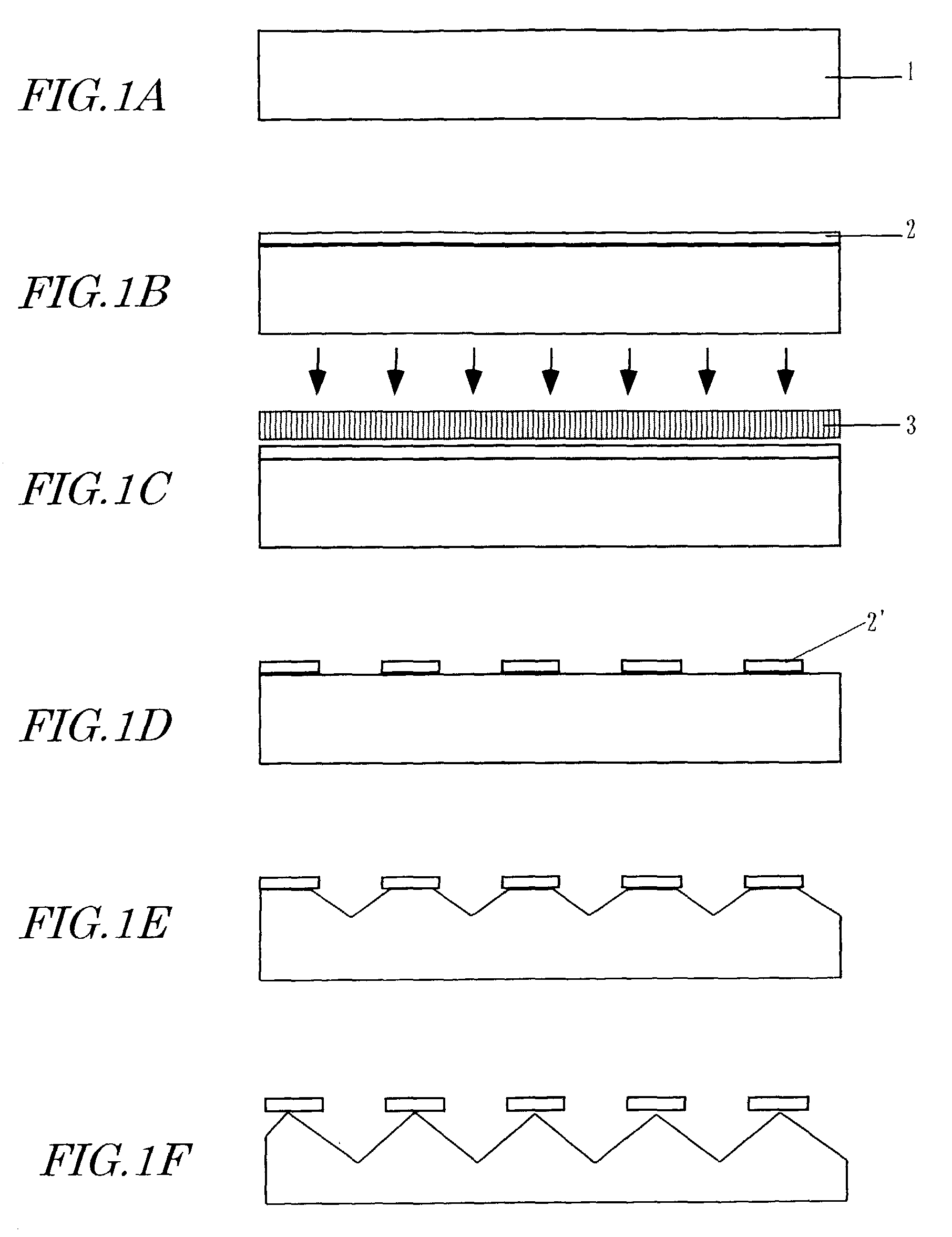
[0152]FIGS. 1A through 1F illustrate respective process steps for making a micro corner cube array according to a first specific preferred embodiment of the present invention. In this preferred embodiment, a single crystalline substrate of GaAs, which is an exemplary compound semiconductor having a sphalerite structure, is used as the cubic single crystalline substrate on which a micro corner cube array should be formed.

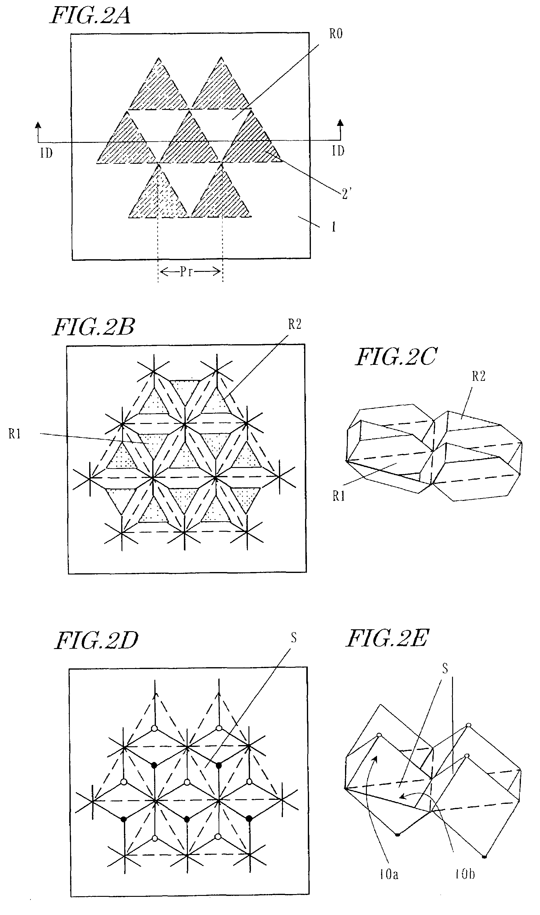
[0153]First, as shown in FIG. 1A, a substrate 1, which consists of GaAs single crystals and of which the surface is one of {111}B planes, is prepared and has that surface mirror-polished. It should be noted that {111}A planes are formed by gallium atoms, while the {111}B planes are formed by arsenic atoms. FIG. 41 shows one of the {111}B planes of GaAs single crystals as viewed from over the substrate 1. In FIG. 41, the configuration of the GaAs crystal unit cell is indicated by the one-dot chains.

[0154]Next, as shown in FIG. 1B, the surface of the substrate 1 is spi...

embodiment 2

[0166]FIGS. 5A through 5I illustrate respective process steps for making a micro corner cube array according to a second specific preferred embodiment of the present invention. In this preferred embodiment, a substrate consisting of germanium single crystals having a diamond structure is used as the cubic single crystalline substrate on which a micro corner cube array should be formed.

[0167]First, in the process step shown in FIG. 5A, a substrate 4, which consists of germanium single crystals and of which the surface is parallel to a (111) plane of the germanium crystals, is prepared and has that surface mirror-polished. Next, an SiO2 layer 5 is deposited by a CVD process, for example, to a thickness of about 200 nm on the mirror-polished surface of the substrate 4. Then, the surface of the SiO2 layer 5 is spin-coated with a positive photoresist layer 2 with a thickness of about 1 μm. The photoresist layer 2 may be made of OFPR-800 (produced by Tokyo Ohka Kogyo Co., Ltd.), for examp...

embodiment 3

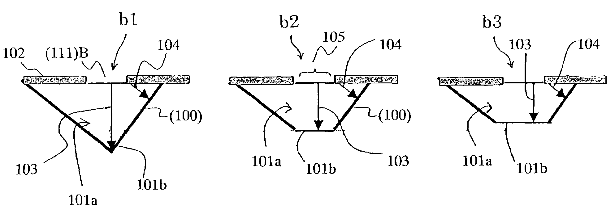
[0180]Hereinafter, a method of making a micro corner cube array according to a third specific preferred embodiment of the present invention will be described. In this third preferred embodiment, a micro corner cube array is also formed on the surface of a single crystalline substrate by subjecting the substrate to an anisotropic etching process as in the first and second preferred embodiments described above. However, in this preferred embodiment, multiple different types of solutions are used as etchants for the anisotropic etching process.

[0181]As shown in FIG. 19A, a GaAs substrate 101 is used as the single crystalline substrate and is selectively covered with an etching mask (i.e., the masking elements of the etching mask layer) 102. Then, the substrate 101 is etched anisotropically though the mask 102, thereby making a micro corner cube array.

[0182]In this preferred embodiment, to investigate exactly how the shape of the resultant micro corner cube array changes with the type o...


PUM

PropertyMeasurementUnit
angleaaaaaaaaaa
angleaaaaaaaaaa
apical angleaaaaaaaaaa

Abstract

A method of making a micro corner cube array includes the steps of: preparing a substrate, at least a surface portion of which consists of cubic single crystals and which has a surface that is substantially parallel to {111} planes of the crystals; and etching the surface of the substrate anisotropically, thereby forming a plurality of unit elements for the micro corner cube array on the surface of the substrate. Each of these unit elements is made up of a number of crystal planes that have been formed at a lower etch rate than the {111} planes of the crystals.

Description

BACKGROUND OF THE INVENTION[0001]1. Field of the Invention[0002]The present invention relates to a micro corner cube array, a method of making the micro corner cube array, and a reflective type display device including the micro corner cube array.[0003]2. Description of the Related Art[0004]In recent years, various types of optical elements having extremely small sizes (i.e., so-called “micro optical elements”), including microlenses, micro mirrors and micro prisms, have been developed and more and more extensively applied to the fields of optical communications and display devices. It is expected that the optical technology and display technology will be further developed and advanced by realizing those micro optical elements.[0005]Examples of such optical elements include a corner cube reflector formed by arranging a plurality of corner cubes in a regular pattern. Each of those corner cubes has a shape corresponding to one corner of a cube and three perpendicularly opposed reflect...

Claims


Application Information

Patent Timeline
Patent Type & Authority Patents(United States)
IPC IPC(8): G02F1/1335G02B5/122G02B5/124G02F1/1334
CPCG02B5/124G02F1/133553G02F1/1334G02F1/1335
Inventor MINOURA, KIYOSHIUEKI, SHUNITOH, YASUHISAIHARA, ICHIROHSAWAYAMA, YUTAKATANIGUCHI, KOHJI
Owner SHARP KK
Why Eureka
Try Eureka