Phase lock loop with coarse control loop having frequency lock detector and device including same

a phase lock and coarse control technology, applied in pulse automatic control, digital transmission, pulse technique, etc., can solve the problems of high noise sensitivity of pll, inability to generate appropriate control signals, and design challenges, and achieve good portability

Active Publication Date: 2006-09-05
LATTICE SEMICON CORP
View PDF1 Cites 80 Cited by
  • Summary
  • Abstract
  • Description
  • Claims
  • Application Information

AI Technical Summary

Benefits of technology

[0019]Some embodiments of the coarse control circuitry of the inventive PLL include digital circuitry for generating coarse control bits, and a DAC for generating a coarse control voltage (for assertion to a VCO) in response to the coarse control bits. When the VCO of the PLL is a ring oscillator including CMOS delay cells connected in a ring structure, use of the DAC allows each of the VCO's delay cells to be implemented much more simply than would be required if the coarse control bits were asserted directly to the VCO's delay cells.
[0021]Another aspect of the invention is a transceiver (e.g., a 10 Gb Ethernet transceiver, typically implemented as or in a single CMOS IC) including a multi-layered receiver interface for receiving and sampling signals, each of the signals being indicative of data having a first data rate (e.g., a four-channel 3.125-Gb / s interface). The receiver interface includes digital circuitry and a single clock-generating PLL: an analog PLL circuit for generating a multiphase clock (to be shared by all layers of the receiver interface). The analog PLL circuit generates all clocks (including the multiphase clock) generated by the receiver interface, or each clock (other than the multiphase clock) generated by the receiver circuitry is generated by circuitry that does not include (and is not) a clock-generating PLL. Each layer of the receiver interface performs blind oversampling on one of the received signals using the multiphase clock. The digital circuitry of the receiver interface includes multilayered digital phase lock loop (DPLL) circuitry which receives the oversampled data. Each layer of the DPLL circuitry effectively selects one phase of the multiphase clock at which one received signal is sampled (by selecting a subset of the oversampled data samples having a “best” phase). The DPLL circuitry typically includes a phase detector (“PD”) that determines a phase error (φΔ) present between each of multiple sampling clocks (determined by the multiphase clock) and data (determined by a received signal) being sampled by each such sampling clock. Because all layers of the receiver interface implement blind oversampling, the digital circuitry (including each layer of the DPLL circuitry) of the receiver interface (and any analog circuitry, other than the analog PLL circuit, of the receiver interface) can share the multiphase clock and / or use clocks derived therefrom. Thus, synchronization is readily achieved between all clocks employed by the receiver interface. When the receiver interface is integrated with additional digital circuitry, and the only analog circuitry in the receiver interface is the shared analog PLL circuit, the digital circuitry of the receiver interface (including the DPLL circuitry) can be synthesized along with the additional digital circuitry, e.g., to achieve good portability.

Problems solved by technology

Such an advanced CMOS technology offers fast transistor speed to achieve 10 Gb / s operation, but also poses design challenges.
Operation of a VCO having high Kvco in a PLL undesirably causes the PLL to have high noise sensitivity, since noise on the power supply and control node is modulated onto the VCO output.
However, if the VCO's frequency-voltage characteristic changes (e.g., as a result of a temperature change or other environmental change) without being affirmatively changed by the coarse control loop, or if the coarse control loop otherwise makes a wrong assumption about the current frequency-voltage characteristic for the VCO, the coarse control loop will infer an incorrect current VCO output frequency from the control voltage measurements and its (incorrect) assumptions about the currently employed frequency-voltage characteristic, and thus will not generate appropriate control signals for controlling the switch positions of the switched-capacitor (SC) network to select a “best” one of the multiple available frequency-voltage characteristics for the VCO.
In this state, another slight change in supply voltage or temperature (lowering the control voltage to below VL without changing the VCO frequency) could cause the FIG. 2 circuitry to execute another compensating change in the frequency-voltage characteristic, resulting in another move of the control voltage to another unstable value (a value slightly below VH), and so on.
However, provision of hysteresis (e.g., by employing additional voltage comparators with reference voltages higher than VH and lower than VL) would have disadvantages (e.g., it could reduce the operating range of a selected frequency-voltage characteristic).
However, the frequency counting method cannot itself resolve the ambiguity as to which one of multiple available frequency-voltage characteristics (all containing the target frequency) should be selected.
However, since the frequency counting method does not measure the actual control voltage, a coarse control loop relying only on the frequency counting method cannot reliably select (as an optimal frequency-voltage characteristic) one of multiple available frequency-voltage characteristics which has the target frequency nearest to the middle of its control voltage range.

Method used


Image

  • Phase lock loop with coarse control loop having frequency lock detector and device including same
  • Phase lock loop with coarse control loop having frequency lock detector and device including same
  • Phase lock loop with coarse control loop having frequency lock detector and device including same

Examples


Embodiment Construction

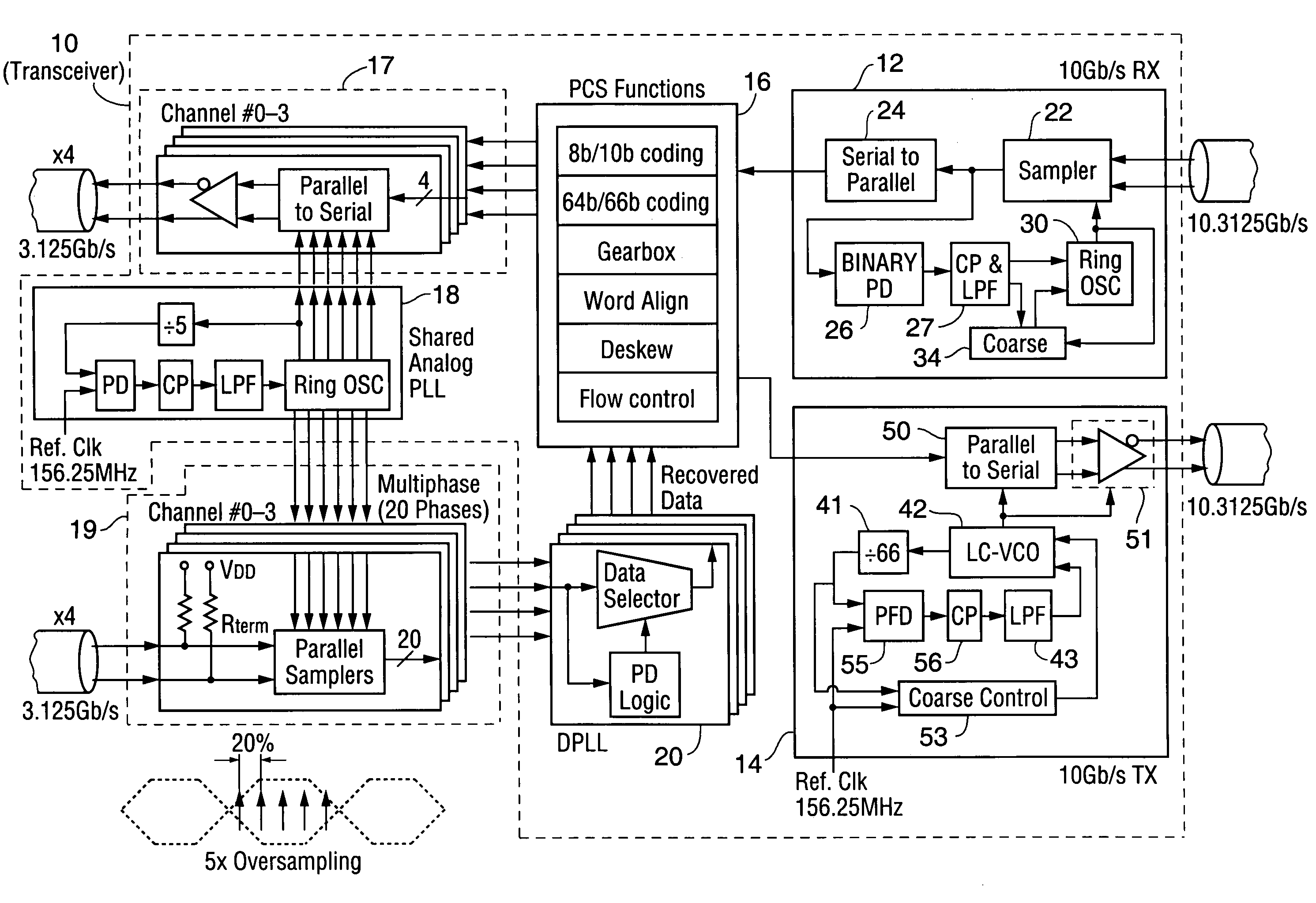
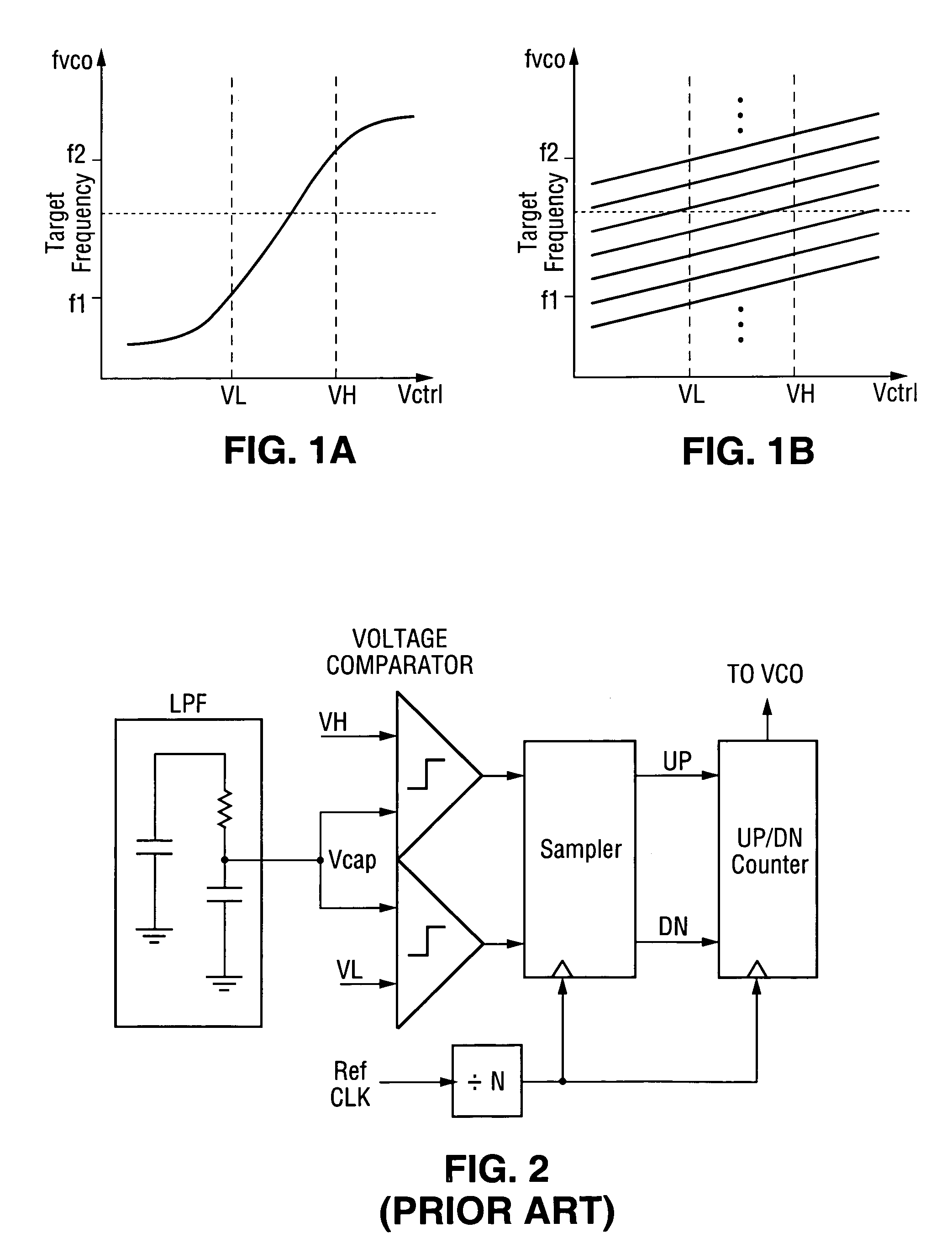
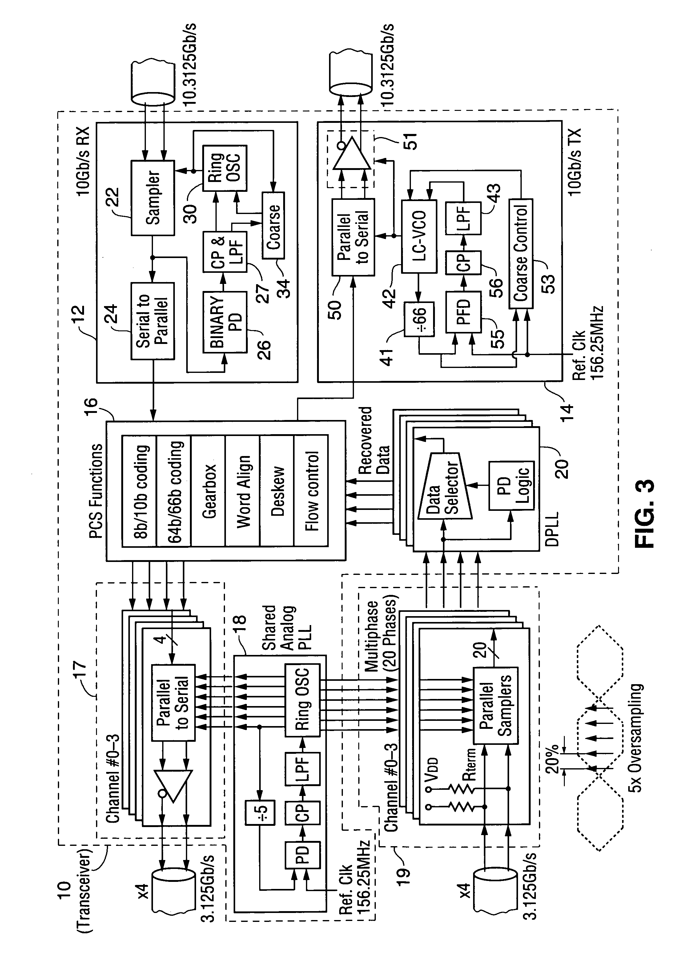
[0053]FIG. 3 is a block diagram of an integrated circuit implementation of a 10 Gb Ethernet transceiver which is an embodiment of the invention. Transceiver chip 10 of FIG. 3 includes a 10.3125 Gb / s Serializer / Deserializer (SerDes) including 10.3125 Gb / s receiver 12 and 10.3125 Gb / s transmitter 14, a four-layer 3.125 Gb / s SerDes including four-layer 3.125 Gb / s transmitter 17, four-layer 3.125 Gb / s receiver 19, and four-layer digital phase lock loop (DPLL) circuitry 20, and physical coding sublayer (PCS) circuitry 16 between the 10.3125 Gb / s SerDes and the 3.125 Gb / s SerDes. Transmitter 14 is configured to transmit over a serial link a differential signal indicative of a bit stream having data rate 10.3125 Gigabits / second. Receiver 12 is configured to receive (from a serial link) and sample a differential signal indicative of a bit stream having data rate 10.3125 Gigabits / second. Transmitter 17 is configured to transmit four differential signals, each over a different serial link, ea...


PUM


Abstract

A phase lock loop (PLL) for controlling a sampling clock or other clock, and a data sampling circuit, transceiver, or other device including such a PLL. The PLL includes a multi-range VCO, at least one fine control loop for controlling the VCO, and a coarse control loop for controlling the VCO by changing its frequency-voltage characteristic. The coarse control loop includes a frequency lock detector and voltage range monitoring logic. Typically, the frequency lock detector locks operation of the coarse control loop when the difference between the VCO output clock frequency and a reference frequency decreases to within a predetermined threshold, and the unlocked coarse control loop employs the voltage range monitoring logic to change the VCO frequency-voltage characteristic when the VCO's fine control voltage leaves a predetermined range. Other aspects are a transceiver (including at least two receiver interfaces and a transmitter interface) implementing a clocking scheme employing no more than three PLLs for clock generation, and a transceiver having a multi-layered receiver interface including digital circuitry and a single clock-generating PLL (an analog PLL for generating a multiphase clock to be shared by all layers of the receiver interface). Each receiver interface layer performs blind oversampling on a different received signal using the multiphase clock and the digital circuitry includes multilayered digital phase lock loop circuitry which receives the oversampled data.

Description

FIELD OF THE INVENTION[0001]The invention pertains to phase lock loop (PLL) circuits and to transceivers, transmitters, receivers, and other devices that include PLL circuits. In some embodiments, the invention pertains to a circuit (e.g., a data sampling circuit) including a PLL circuit (having both coarse control and fine control loops) for controlling the phase of a clock (e.g., a sampling clock), and to a device (e.g., an 10 Gb Ethernet transceiver) including such a PLL circuit.BACKGROUND OF THE INVENTION[0002]The term “transceiver” is used herein to denote any device that performs the functions of a transmitter and a receiver. The term “transmitter” is used herein in a broad sense to denote any device capable of transmitting data over a link (e.g., a serial link), and optionally also capable of performing additional functions which can include encoding and / or encrypting the data to be transmitted. The term “receiver” is used herein in a broad sense to denote any device capable ...

Claims


Application Information

Patent Timeline
Patent Type & Authority Patents(United States)
IPC IPC(8): H03L7/07H03L7/087H04B1/40H04B1/50
CPCH03K23/507H03L7/087H03L7/089H03L7/093H03L7/0995H03L7/10H04L7/0337H03L7/099Y10S331/02H03L2207/06H03L7/103
Inventor LEE, HYUNG-ROKHWANG, MOON-SANGLEE, SANG-HYUNLEE, BONG-JOONJEONG, DEOG-KYOON
Owner LATTICE SEMICON CORP
Why Eureka
Try Eureka