
Logic and memory device integration

a logic and memory device technology, applied in the direction of micro-instruction address formation, instruments, sustainable buildings, etc., can solve the problems of non-buffered signal lines that are substantially incapable of level translation and may further be non-buffered, so as to reduce the size of the circuit, reduce the power requirement, and eliminate or reduce certain redundant circuits

Inactive Publication Date: 2006-09-05
ROUND ROCK RES LLC
View PDF9 Cites 1 Cited by
  • Summary
  • Abstract
  • Description
  • Claims
  • Application Information

AI Technical Summary

Benefits of technology

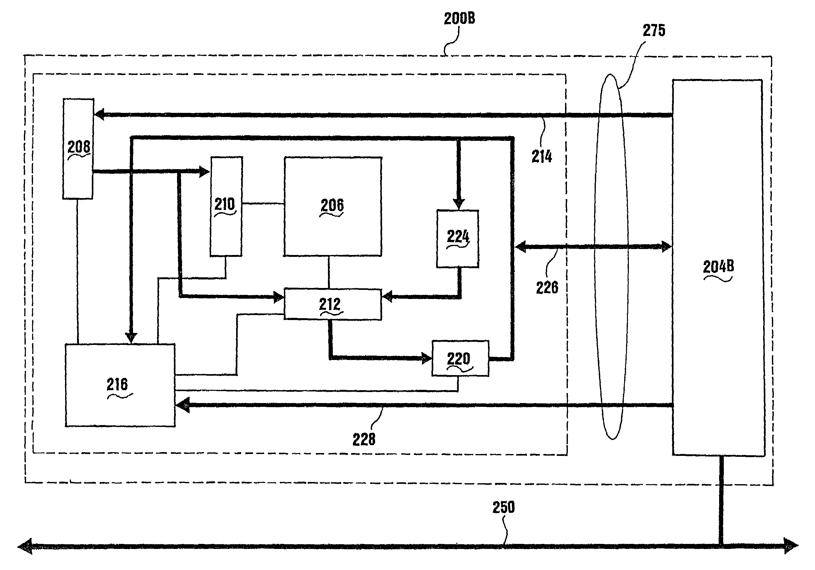
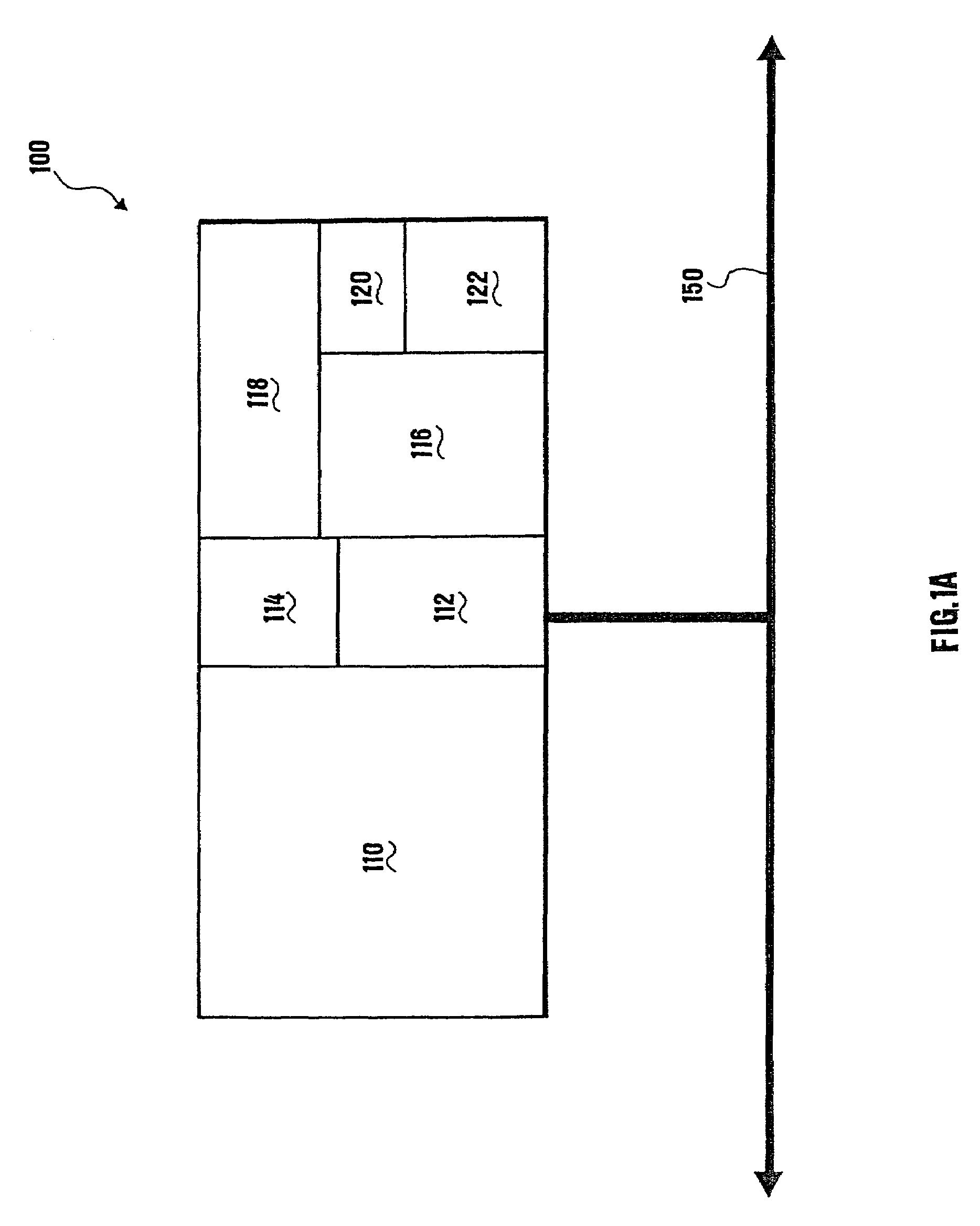
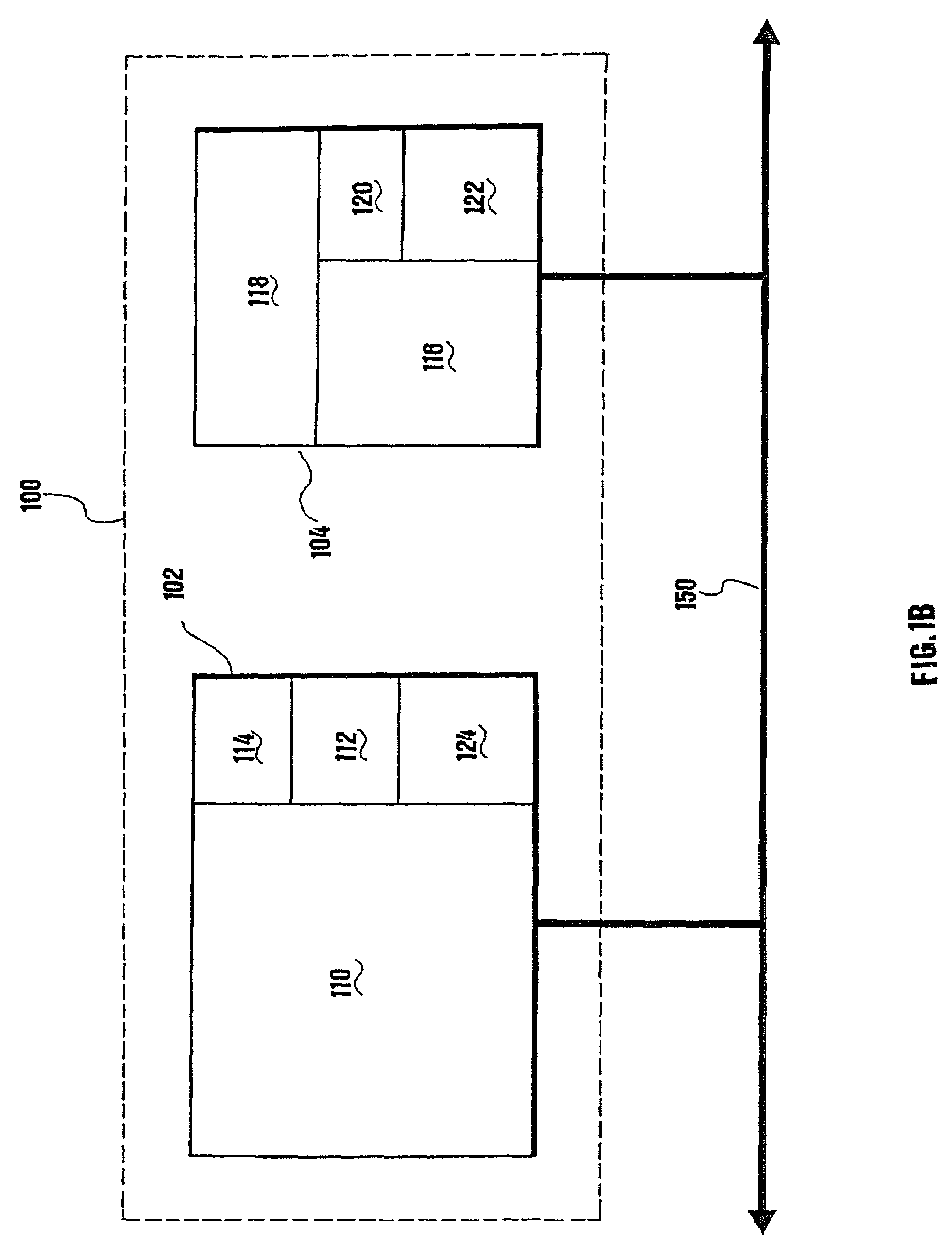
[0014]Memory devices of the type described herein are capable of lower power requirements and reduced size due in part to the elimination or reduction of certain redundant circuitry. Direct interfacing through the local bus facilitates the elimination or reduction of input / output (I / O) buffer circuitry by eliminating the need to step up to and step down from typical system bus voltage levels. Such memory devices thus require less semiconductor die area and have lower power demand due to the elimination or reduction of the buffer circuitry. Direct interfacing through the local bus may further facilitate lower power requirements and reduced size of the output driver circuitry; the output driver circuitry need only drive power levels compatible with internal logic demands of the logic device over a dedicated local bus rather than drive power levels to overcome the power dissipation associated with a general-purpose system bus.

Problems solved by technology

The nominally-buffered signal line is substantially incapable of level translation and may further be non-buffered.

Method used


Image

  • Logic and memory device integration
  • Logic and memory device integration
  • Logic and memory device integration

Examples


Embodiment Construction

[0025]In the following detailed description of the present embodiments, reference is made to the accompanying drawings that form a part hereof, and in which is shown by way of illustration specific embodiments in which the invention may be practiced. These embodiments are described in sufficient detail to enable those skilled in the art to practice the invention, and it is to be understood that other embodiments may be utilized and that process, electrical or mechanical changes may be made without departing from the scope of the present invention. The terms wafer or substrate used in the following description includes any base semiconductor structure. Examples include silicon-on-sapphire (SOS) technology, silicon-on-insulator (SOI) technology, thin film transistor (TFT) technology, doped and undoped semiconductors, epitaxial layers of a silicon supported by a base semiconductor structure, as well as other semiconductor structures well known to one skilled in the art. Furthermore, wh...


PUM


Abstract

Memory devices are adapted for direct interface or virtual integration with a processor or other logic device through a local bus and isolated from a system bus. Such memory devices are capable of lower power requirements and reduced size due in part to the elimination of certain redundant circuitry. Direct interfacing through the local bus facilitates the elimination or reduction of input / output (I / O) buffer circuitry by eliminating the need to step up to and step down from typical system bus voltage levels. Communication between the memory device and a separate logic device occurs across the local bus at voltage levels compatible with internal logic levels of the memory device.

Description

TECHNICAL FIELD OF THE INVENTION[0001]The present invention relates generally to semiconductor memory devices, and in particular, the present invention relates to semiconductor memory devices designed for integration with a processor or other logic device and systems produced therefrom.BACKGROUND OF THE INVENTION[0002]Electronic information handling or computerized systems, whether large machines, microcomputers or small handheld devices, require memory for storing data and program instructions. Various memory systems have been developed over the years to address the evolving needs of information handling systems. One such memory system includes semiconductor memory devices.[0003]Semiconductor memory devices are rapidly-accessible memory devices. In a semiconductor memory device, the time required for storing and retrieving information generally is independent of the physical location of the information within the memory device. Semiconductor memory devices typically store informati...

Claims


Application Information

Patent Timeline
Patent Type & Authority Patents(United States)
IPC IPC(8): G11C5/06G11C7/00G06F13/40
CPCG06F13/4072Y02B60/1235Y02B60/1228Y02D10/00
Inventor FAZIO, MARIO
Owner ROUND ROCK RES LLC
Learn More