Method of manufacturing a semiconductor device

a manufacturing method and semiconductor technology, applied in semiconductor/solid-state device testing/measurement, identification means, instruments, etc., can solve the problems of inability to reduce time and cost, inability to confirm the presence of defects, and inability to reduce packaging and attaching connector processes, so as to prevent a decrease in yield, the inspection process is simplified, and the suitability of a tft substrate for a product can be confirmed.

Inactive Publication Date: 2006-09-12
SEMICON ENERGY LAB CO LTD
View PDF13 Cites 145 Cited by
  • Summary
  • Abstract
  • Description
  • Claims
  • Application Information

AI Technical Summary

Benefits of technology

[0018]According to the present invention, due to the above-mentioned configuration, the suitability of a TFT substrate for a product can be confirmed without directly connecting a probe to the TFT substrate. Therefore, a defect generated by minute dust that adheres to the TFT substrate during an inspection process is reduced, which can prevent a

Problems solved by technology

It is difficult to confirm the presence of a defect until an EL display is completed and a display is actually conducted, even if there is some inconvenience in circuits or circuit elements for controlling light emission of a light-emitting element.
In this case, the processes of forming a light-emitting element, packaging, and attaching a connector become useless, so that time and cost cannot be reduced.
Furthermore, even in the case of forming an EL panel using a multiple-chamfered substrate, the processes of packaging and attaching a conne

Method used


Image

  • Method of manufacturing a semiconductor device
  • Method of manufacturing a semiconductor device
  • Method of manufacturing a semiconductor device

Examples


embodiment mode 1

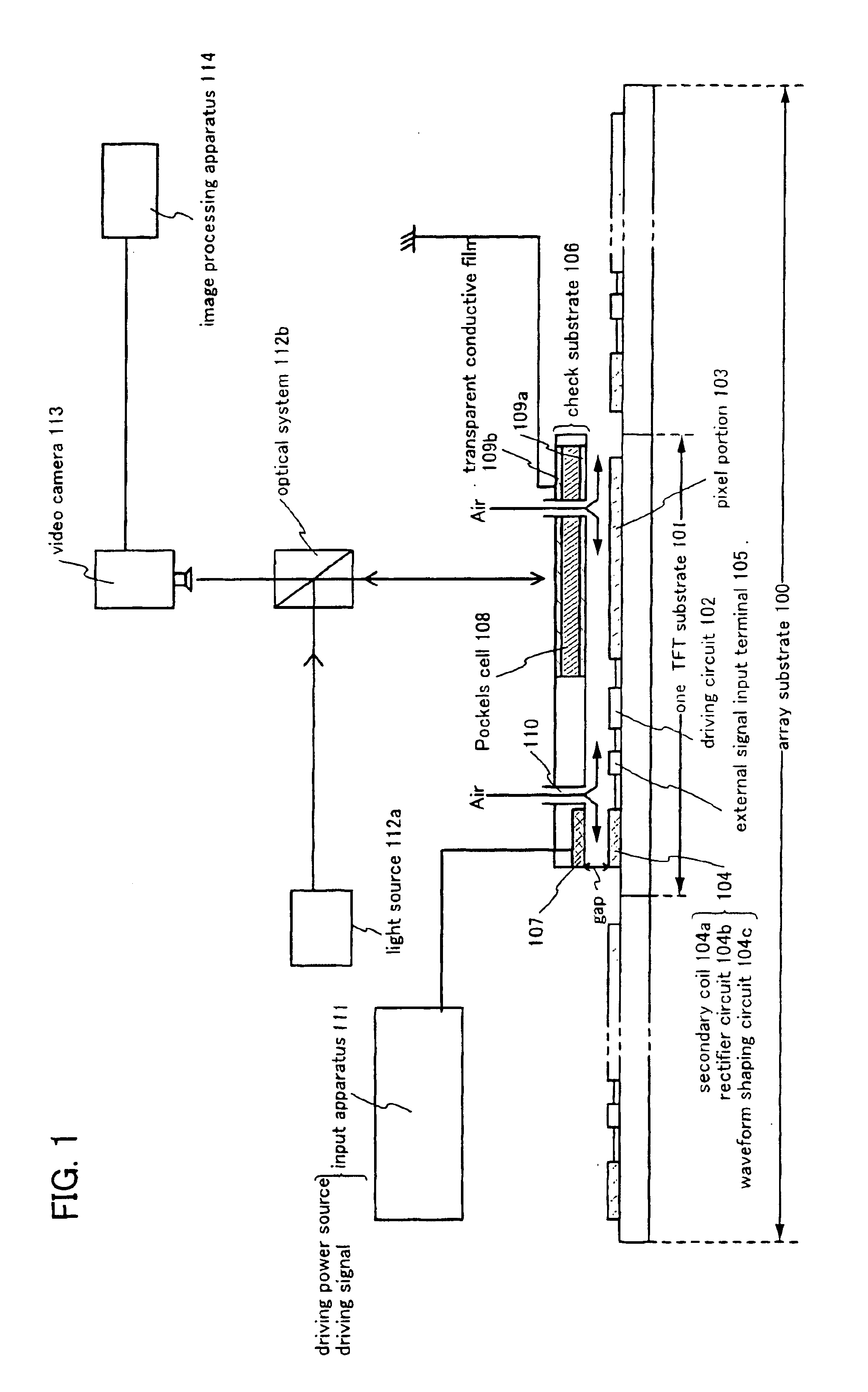
[0043]In the present embodiment mode, a process of manufacturing a plurality of TFT substrates 101 on an array substrate 100, an inspection process of confirming the quality of manufactured TFT substrates, and a process of forming light-emitting elements on the TFT substrates that are determined to be satisfactory will be described with reference to FIGS. 1 to 5, and FIGS. 20A-B to 23A-23C.

[0044]In the present embodiment mode, the case of forming a light-emitting element on a TFT substrate will be described. However, the present invention is applicable not only to a light-emitting device (EL display) having a light-emitting element, but also to all the electric equipment using a semiconductor element which uses semiconductor characteristics, such as a liquid crystal display device, for example, a transistor, in particular, a field-effect transistor; typically, a MOS (Metal Oxide Semiconductor) transistor and a TFT (Thin Film Transistor).

[0045]First, driving circuits 102 including TF...

embodiment mode 2

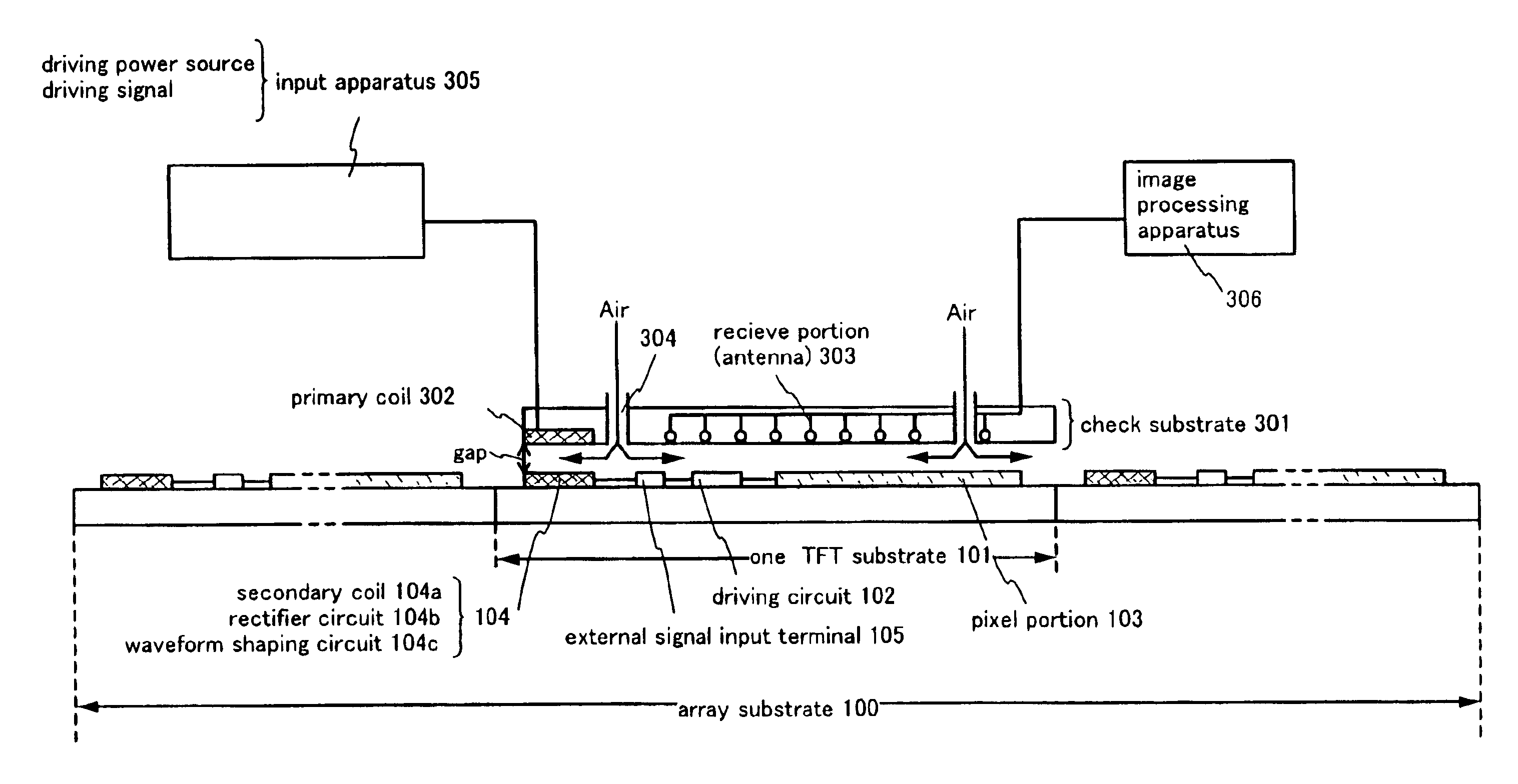
[0099]In the present embodiment mode, another inspection method for a TFT substrate will be described with reference to FIGS. 4A and 4B and 6.

[0100]When circuits or circuit elements on a TFT substrate formed on an array substrate are operated, an electromagnetic wave is generated. According to the inspection method disclosed in the present embodiment mode, by measuring the intensity and frequency of the electromagnetic wave, and the intensity and frequency of the electromagnetic wave on the basis of a certain period of time, it is confirmed if a TFT substrate is suitable for a product.

[0101]The intensity and frequency of an electromagnetic wave of a circuit on a TFT substrate determined to be satisfactory (suitable for a product), and the intensity and frequency thereof on the basis of a certain period of time may be previously measured and used for comparison for determining the suitability of a TFT substrate for a product.

[0102]Then, circuits or circuit elements on a TFT substrate...

embodiments

Embodiment 1

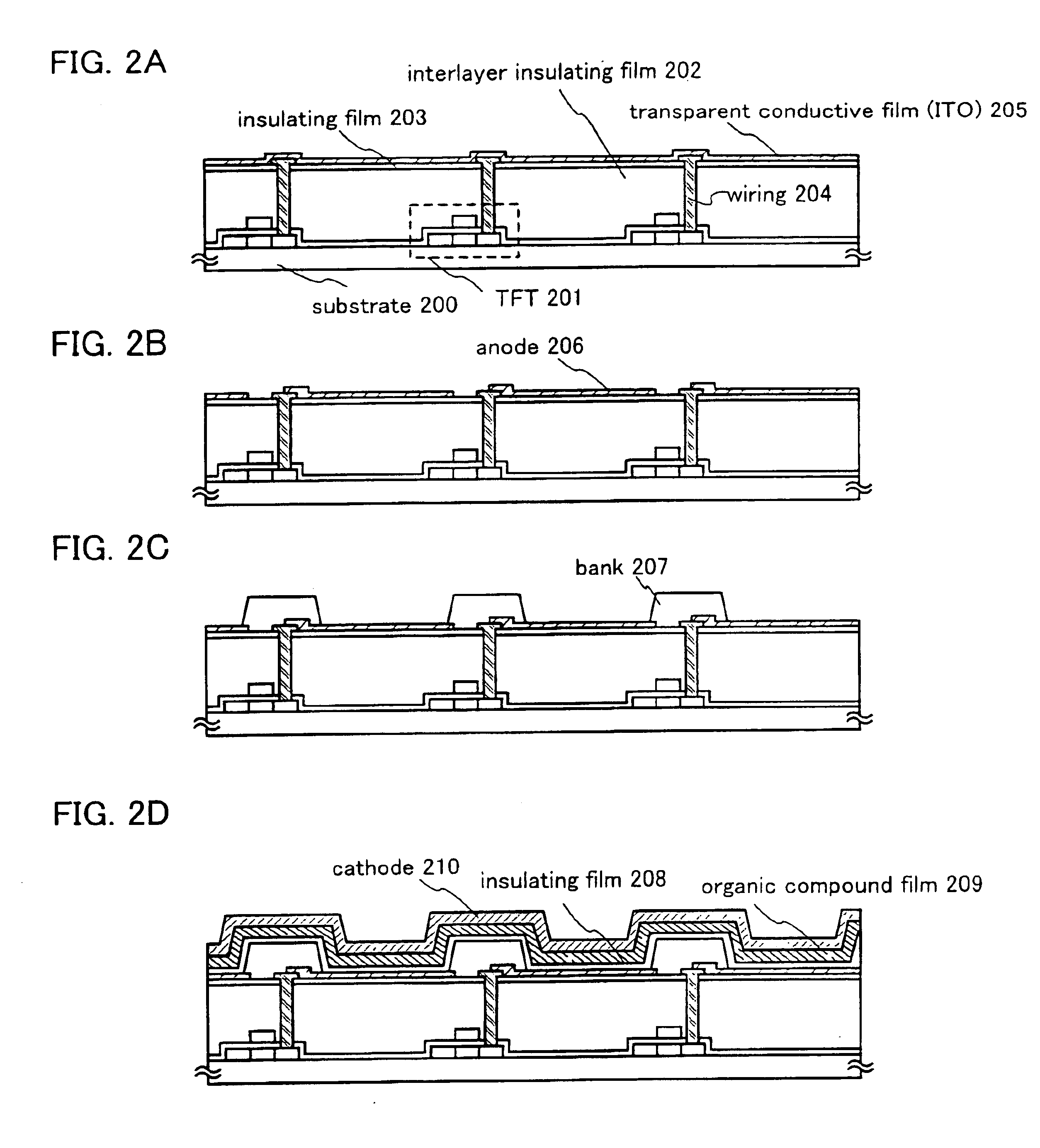
[0113]In the present embodiment, a light-emitting element manufactured according to the present invention will be described. Herein, an example of a method of manufacturing a pixel portion having a light-emitting element of the present invention, TFTs (an n-channel TFT and a p-channel TFT) of a driving circuit provided on the periphery of the pixel portion, a secondary coil of a transformer, a rectifier circuit and a waveform shaping circuit for inspecting driving of a TFT substrate on the same substrate will be described with reference to FIGS. 7A-7D to 10A and 10B.

[0114]First, in the present embodiment, a substrate 900 made of glass such as barium borosilicate glass or aluminoborosilicate glass, which is represented by #7059 glass and #1737 glass produced by Corning Co., is used. As the substrate 900, any substrate having transparency can be used, and a quartz substrate may be used. Furthermore, a plastic substrate having heat resistance withstanding a treatment temper...


PUM


Abstract

The present invention supplies a manufacturing method of a semiconductor device, which includes a non-contact inspection process capable of confirming if a circuit or circuit element formed on an array substrate is normally performed and can decrease a manufacturing cost by eliminating wastes to keep a defective product forming.
An electromotive force generated by electromagnetic induction is rectified and shaped by using primary coils formed on a check substrate and secondary coils formed on an array substrate, whereby a power source voltage and a driving signal are supplied to circuits or circuit elements on a TFT substrate so as to be driven.

Description

BACKGROUND OF THE INVENTION[0001]1. Field of the Invention[0002]The present invention relates to a method of manufacturing a semiconductor device including an inspection process of a semiconductor element that uses semiconductor characteristics (e.g., a transistor, in particular, a field-effect transistor; typically, a metal oxide semiconductor (MOS) transistor and a thin film transistor (TFT)). More specifically, the present invention relates to a non-contact type inspection apparatus and an inspection method using the same. The present invention also relates to a method of manufacturing a semiconductor device including an inspection process of such a semiconductor element.[0003]2. Description of the Related Art[0004]In an active matrix type liquid crystal display and an electroluminescence (EL) display, a TFT is generally provided in each pixel. In the case of a liquid crystal display, one TFT formed in each pixel functions as a switching element. In the case of an EL display, amo...

Claims


Application Information

Patent Timeline
IPC IPC(8): H01L21/66G01R31/26G02F1/1368G09F9/00G09G3/00H01L21/336H01L21/77H01L21/84H01L27/12H01L27/13H01L29/786
CPCH01L27/1255G09G3/00G01R31/3025G09G3/006H01L22/00G01R31/2601G01R31/2607H01L22/14
Inventor HIROKI, MASAAKIYAMAZAKI, SHUNPEI
Owner SEMICON ENERGY LAB CO LTD
Why Eureka
Try Eureka