Analogue to digital converter

a converter and digital technology, applied in the field of analog to digital converters, can solve the problems of increasing the cost of dies, inherently more difficult to achieve, and presenting greater design challenges for pga op amps

Active Publication Date: 2006-09-12
CIRRUS LOGIC INC
View PDF4 Cites 31 Cited by
  • Summary
  • Abstract
  • Description
  • Claims
  • Application Information

AI Technical Summary

Benefits of technology

[0075]An aspect of the invention improves previous embodiments of recirculating or algorithmic ADCs by incorporating the use of capacitors and switches into an ADC to allow the use of only one amplifier such as an op amp in the ADC, while still allowing most of a sample period for the corresponding PGA to settle into the ADC input.
[0076]Another aspect of the invention provides a recirculating ADC with two feedback units for use with a single amplifier such as an op amp, characterised by a third feedback unit to be used in an initial step with the initial sample. In that way, settling time as a proportion of the whole conversion cycle can be reduced.

Problems solved by technology

The PGA op amp can often present greater design challenges than the ADC op amps.
This is inherently more difficult to achieve than in an ADC, which has a closed loop gain of, for example, 2, thus requiring a gain bandwidth of 60 MHz and only needing to be stable for constant gain A=2.
This uses significant silicon area, each stage adding to die cost, but these ADCs are often required in high-volume consumer equipment, where manufacturing cost is very important.
Also each stage consumes power, whereas many applications such as Digital Cameras are battery-powered portable equipment, so low power is important.
Pipeline ADCs extracting more than one bit per stage have fewer stages, but each is more complex, consuming more area and more power per stage, so the net saving in terms of power and area is limited.
The main problem is that the PGA now has to drive the input capacitors in a small fraction of the 3 Ms / s sample rate.
This arrangement has the disadvantage that, unless the input offset of the flash ADC comparator is less than 1LSB (for 14 bits, Vref=1V, 1LSB=1V / 16384=60 μV, which is impractical in terms of offset voltage and overdrive required for reasonable response time), the extreme outputs of stage 1 will exceed or not get to the full-scale input range of the subsequent processing, so the whole pipeline ADC will exhibit missing or duplicate codes as the input is swept over the signal range.
However, incomplete settling of the op amp, in conjunction with parasitic capacitances on that node, may lead to some residual virtual earth signal charge propagating from one phase to the next.
Assuming settling to less than 1LSB at the output, and parasitic capacitances smaller than the signal capacitances, this effect will be negligible during a few conversions, but over thousands of conversions the resulting errors might accumulate.
Further, there will be some small but non-zero leakage currents associated with real switches on this node.
Some improvement could be obtained by stretching the on-time of the initial phase comprising φ2x but, for a given input sample rate, this implies decreasing the time for the remaining conversion phases, so only limited improvement is available without reducing the available settling time for the later stages to well below 16.7 ns.

Method used


Image

  • Analogue to digital converter
  • Analogue to digital converter
  • Analogue to digital converter

Examples


Embodiment Construction

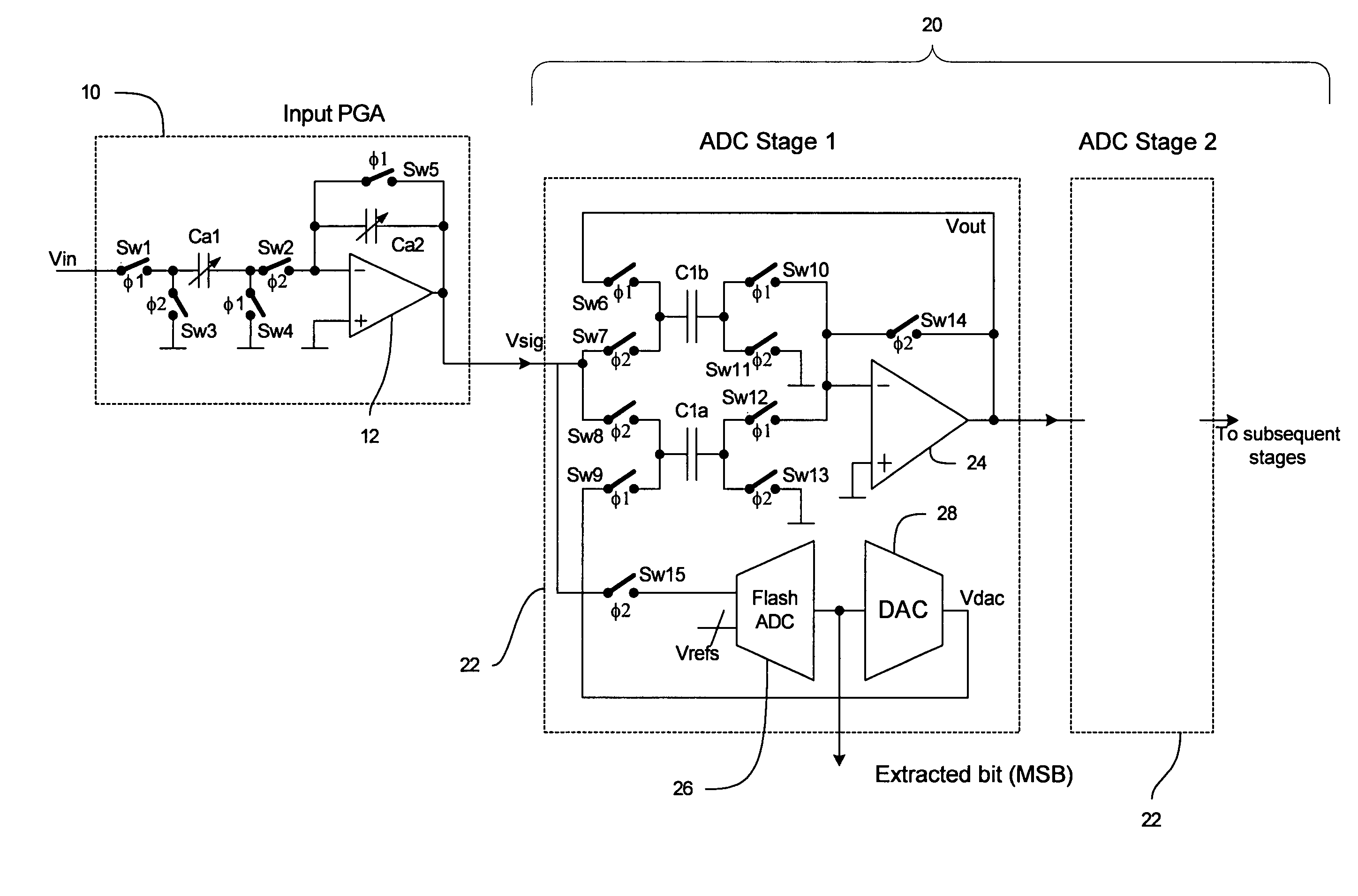
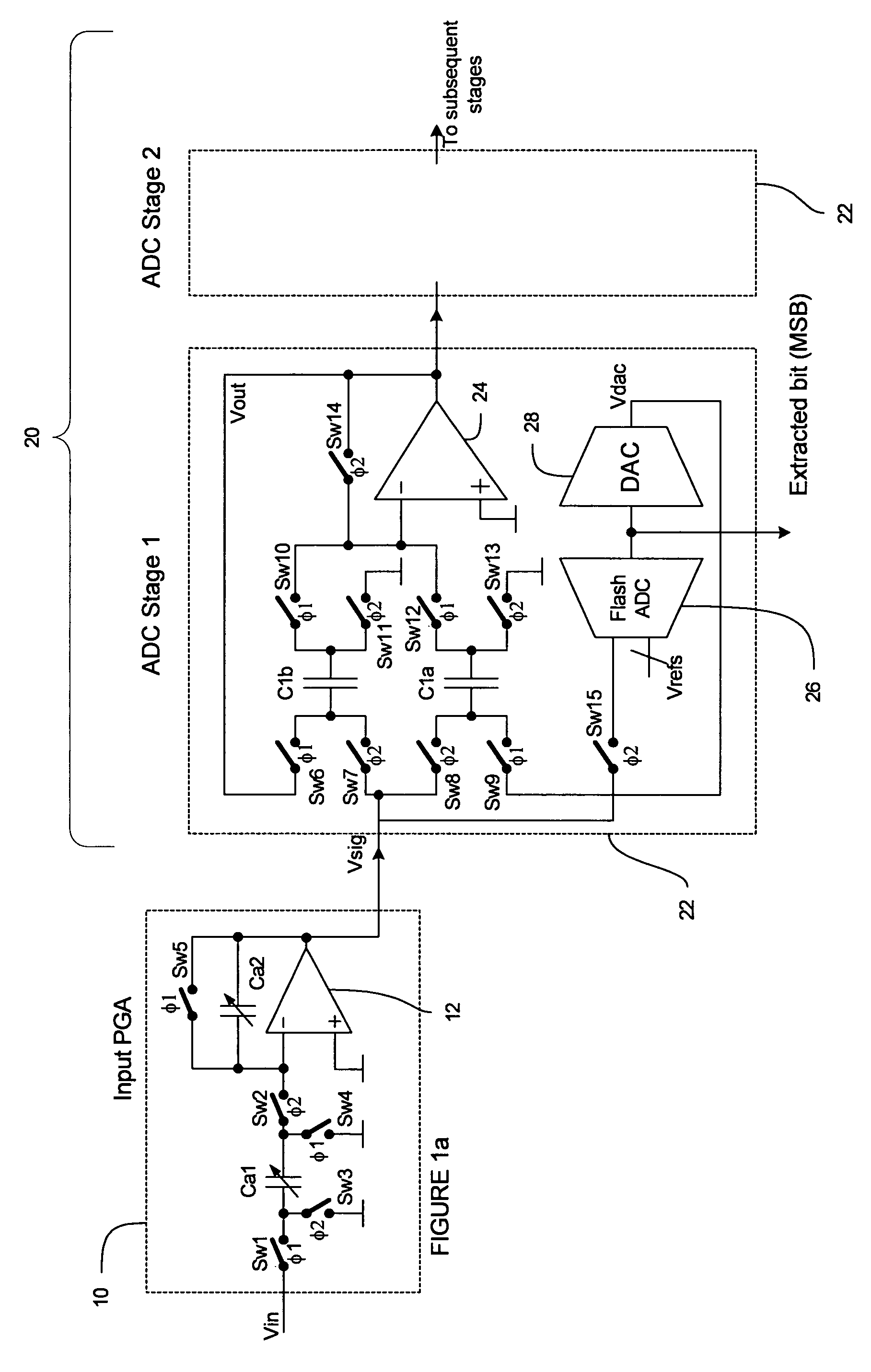
[0095]The circuit of FIG. 6 shows a recirculating stage of an ADC, similar to that illustrated in FIG. 4, but with functional and operational distinctions. Table 1 illustrates a correspondence between the functional equivalence of certain of the switches of the arrangement of FIG. 4 and that of FIG. 6.

[0096]

TABLE 1FIG. 4FIG. 6Sw52Sw84Sw53Sw85Sw54Sw86Sw55Sw87Sw56Sw92Sw59Sw97Sw61Sw98Sw62Sw80Sw63Sw81Sw64Sw82Sw65Sw83Sw66Sw88Sw67Sw89Sw68Sw90Sw69Sw91Sw70Sw101

[0097]The structural difference is that the φ2 switches (Sw57, Sw58, Sw60) that were connected to C1a, C1b and the flash ADC, in series with other switches (Sw50, Sw51) driven by φ2x, φ2y respectively have been replaced by parallel switches (Sw93, Sw94; Sw95, Sw96; Sw99, Sw100) connected to φ2x, φ2y. Since φ2 is equivalent to φ2x.OR.φ2y, this connection is equivalent. The total number of switches is increased by one, but each switch can be of higher on-resistance and thus occupy less area.

[0098]An advantage of this arrangement is that...


PUM


Abstract

An analogue to digital converter (ADC) of the recirculating type is described. In one embodiment, the ADC is composed of three storage and residual determination units, which, in cooperation with an operational amplifier, and suitable comparator means, are operable to re-present residual signals for analogue to digital conversion. To enhance settling at the beginning of a cycle, the first storage and residual determination unit is used once, with remaining recirculation being conducted between the other two storage and residual determination units.Another embodiment presents a recirculating ADC stage which comprises a plurality of capacitor banks operable to be switched into and out of connection with other components of the ADC stage, in order to recirculate residual values for calculation of further bits of a digital output. Each bank comprises a plurality of capacitors, and cooperating switching means for connecting each bank in turn with the other components. The switching means are controlled by timing signals, wherein the switching means for each capacitor in each capacitor bank interpose the same number of switches between that capacitor and fed-back signals to that capacitor as to other capacitors of that bank.

Description

FIELD OF THE INVENTION[0001]This invention relates to an Analogue to Digital Converter-(ADC), and particularly to a recirculating or algorithmic ADC.BACKGROUND OF THE INVENTION[0002]Pipeline ADCs are today commonly used for applications requiring 10 to 16 bits resolution at 1 MHz to 100 MHz sample rates, for example for digitising the outputs of CCD or CMOS linear or area image sensors or for digitising analogue video signals. A basic pipeline ADC includes several stages in cascade. Each stage uses a comparator to extract the most significant bit, and then the stage subtracts an analogue signal corresponding to the extracted bit, and amplifies the remaining residue, for use by the next stage. Commonly, more than one bit per stage is extracted, by using multiple comparators. Also, certain arrangements allow over-ranging of the input of each stage to accommodate comparator offsets so that, provided that each stage subtracts an accurate amount and gives an accurate analogue gain, the e...

Claims


Application Information

Patent Timeline
Patent Type & Authority Patents(United States)
IPC IPC(8): H03M1/34H03M1/16H03M1/18H03M1/40
CPCH03M1/1215H03M1/403
Inventor CRINGEAN, ANDREW J.
Owner CIRRUS LOGIC INC
Why Eureka
Try Eureka