Memory system using non-distributed command/address clock signals

a clock signal and memory technology, applied in the field of memory systems, can solve the problems of increasing jitter and cost of the whole system, complicated semiconductor device design, and generating clock domain collisions between clocks and write data capture clocks, so as to improve jitter performance, simplify semiconductor device design, and reduce cost

Inactive Publication Date: 2006-09-12
SK HYNIX INC
View PDF9 Cites 6 Cited by
  • Summary
  • Abstract
  • Description
  • Claims
  • Application Information

AI Technical Summary

Benefits of technology

[0007]In order to overcome the above described problems, the present invention has an object to provide a memory system which simplifies the lay-out of semiconductor device design by removing transmission lines for distributing command / address clocks CACLK, prevents clock domain collision by sampling command / address signals according to write data capture clocks WCLKs or clock signals divided into integer multiple, reduces cost without requiring an individual PLL or DLL circuit, improves jitter performance and prevents degradation of timing margins of system due to differences of compensation capacitor.
[0008]A preferred embodiment of the present invention has an object to provide a memory system for reducing cost due to unification of register chip, PLL or DLL chips.

Problems solved by technology

However, the conventional memory system has the following problems.
First, since the conventional memory system should include the transmission lines to transmit clocks CLK0–CLK3 to the plurality of memory devices, the lay-out of semiconductor device design becomes complicated.
Second, since the memory devices receive clocks CLK0–CLK3 and write data capture clocks ‘WCLK’, clock domain collision can be generated between clocks and write data capture clocks.
Third, since each memory device should comprise an individual PLL or DLL circuit, jitter and cost of the whole system are increase.
Fourth, since a register and a PLL circuit should be embodied using separate chips, the packaging process of semiconductor devices is complicated, thereby the packaging cost is increased.

Method used


Image

  • Memory system using non-distributed command/address clock signals
  • Memory system using non-distributed command/address clock signals
  • Memory system using non-distributed command/address clock signals

Examples


Embodiment Construction

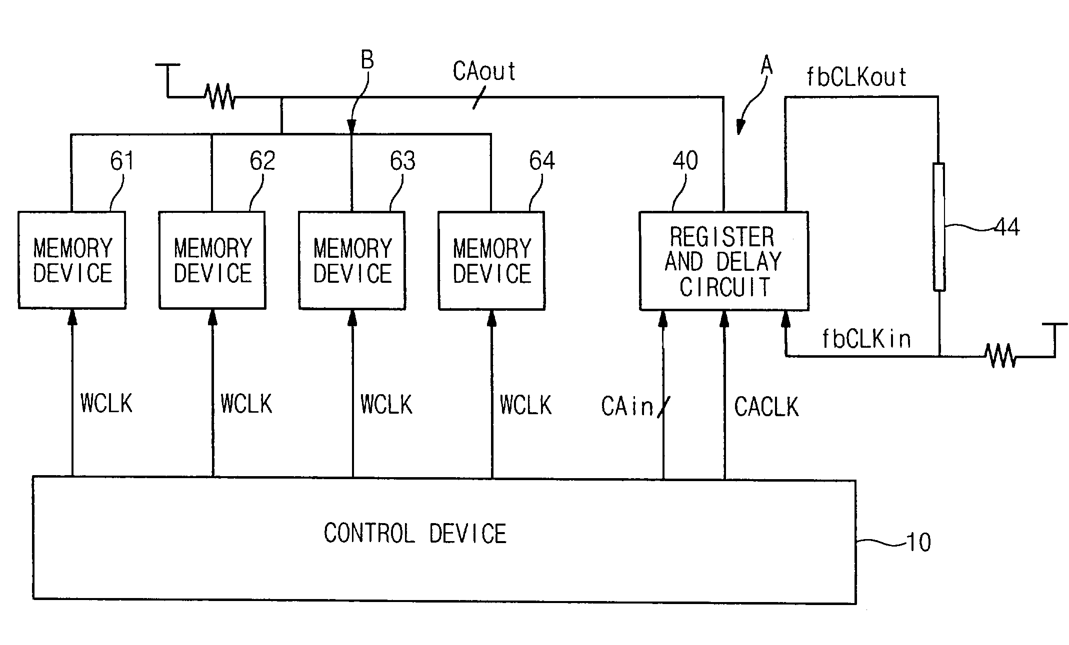
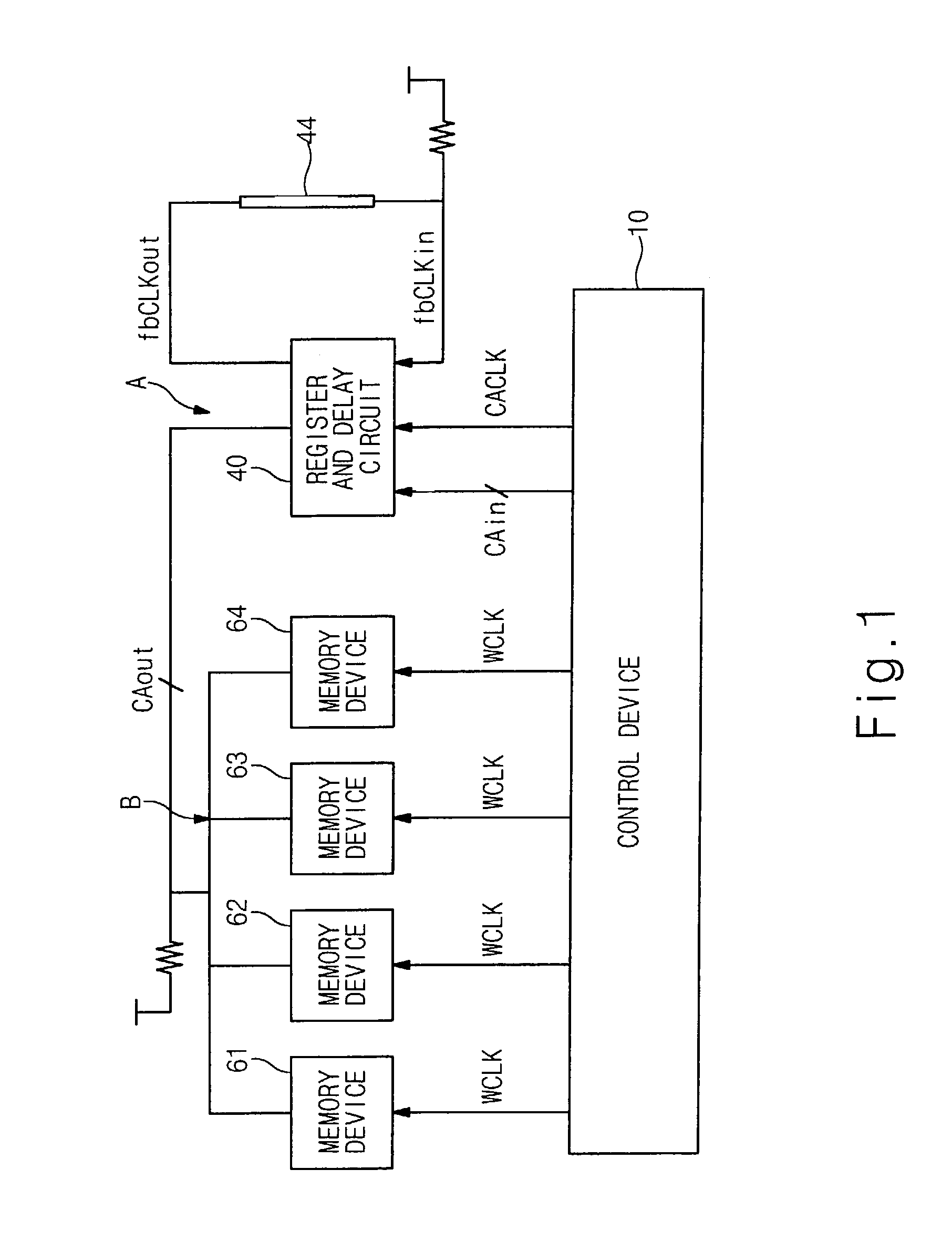
[0012]A disclosed memory system comprising a plurality of memory devices includes: a controller for outputting a first clock signal, a second clock signal and a plurality of command / address input signals to the plurality of memory devices, respectively; and a register and delay circuit unit for outputting command / address output signals after receiving the command / address input signals from the controller and then correcting transmission delay due to transmission lines; wherein the plurality of memory devices receive the command / address output signal from the register and delay circuit unit via the transmission lines, respectively, and sample the command / address output signals using the first clock signal directly inputted from the controller.

[0013]The disclosed memory system comprising a plurality of memory devices will be described in more details referring to examples below, when are not intended to be limiting.

[0014]FIG. 1 is block diagram of a memory system in accordance with a ...


PUM


Abstract

A memory system that includes a plurality of memory devices includes: a controller for outputting a first clock signal, a second signal and a plurality of command/address input signals corresponding to the plurality of memory devices, respectively; and a register and delay circuit unit for outputting command/address output signals after receiving the command/address input signals front the controller and then correcting transmission delay due to transmission lines; wherein the plurality of memory devices receive the command/address output signals from the register and delay circuit unit via the transmission lines, respectively, and sample the command/address output signals using the first clock signal directly inputted from the controller. As a result, the memory system can simplify the layout of semiconductor device design and prevent the collision of clocks.

Description

BACKGROUND OF THE INVENTION[0001]1. Field of the Invention[0002]The present invention generally relates to memory systems comprising a plurality of memory devices, and more particularly, to a memory system for removing a command / address clock which samples command / address signals is removed.[0003]2. Description of the Prior Art[0004]A clock control device of conventional memory devices comprises a register chip for buffering command / address input signals and a phase locked loop chip for generating timing signals, in case of dual in line memory module ‘DIMM’. When a plurality of PLL output clocks are generated in the PLL, a compensation capacitor (hereinafter, referred to as ‘Ccomp’) is used to control their edge timing.[0005]FIG. 3 is a diagram illustrating an example of a conventional memory system using distributed command / address signals. A PLL circuit 20 edge controls address clocks ‘CACLK’ inputted from a controller 10 by using the Ccomp, which compensates signal delay generate...

Claims


Application Information

Patent Timeline
Patent Type & Authority Patents(United States)
IPC IPC(8): G06F1/04G11C8/00G06F12/00G06F13/16G06F13/42G11C7/00
CPCG06F13/4243
Inventor JEONG, YONG GWONKWON, CHANG KI
Owner SK HYNIX INC
Why Eureka
Try Eureka