Light-emitting semiconductor device using group III nitride compound

a technology of light-emitting semiconductors and nitride compounds, which is applied in semiconductor devices, semiconductor/solid-state device details, electrical devices, etc., can solve the problems of device not obtaining an adequate luminous intensity as a light-emitting semiconductor device, insufficient reflectivity of visible (violet, blue, green) rays whose wavelength is in the range of 380 nm to 550 nm, and persisting luminous intensity, etc., to achiev

Inactive Publication Date: 2006-09-19
TOYODA GOSEI CO LTD
View PDF73 Cites 71 Cited by
  • Summary
  • Abstract
  • Description
  • Claims
  • Application Information

AI Technical Summary

Benefits of technology

[0008]Another object of the present invention is to obtain a light-emitting semiconductor device whose electrode has a high reflectivity and a high durability and in which the structure of electrodes is simplified.
[0040]The flip chip type of light-emitting semiconductor device shown in the fifteenth aspect of the present invention differs from that of the thirteenth and the fourteenth aspect of the present invention int eh constituent elements of the second and the third positive electrode layers. The semiconductor device shown in the fifteenth aspect can provide the same effect as that shown in the thirteenth and the fourteenth aspect of the present invention.

Problems solved by technology

However, a problem persists in luminous intensity.
As a result, a reflectivity of visible (violet, blue, and green) rays whose wavelength is in the range of 380 nm to 550 nm was insufficient, and the device could not obtain an adequate luminous intensity as a light-emitting semiconductor device.

Method used


Image

  • Light-emitting semiconductor device using group III nitride compound
  • Light-emitting semiconductor device using group III nitride compound
  • Light-emitting semiconductor device using group III nitride compound

Examples


first embodiment

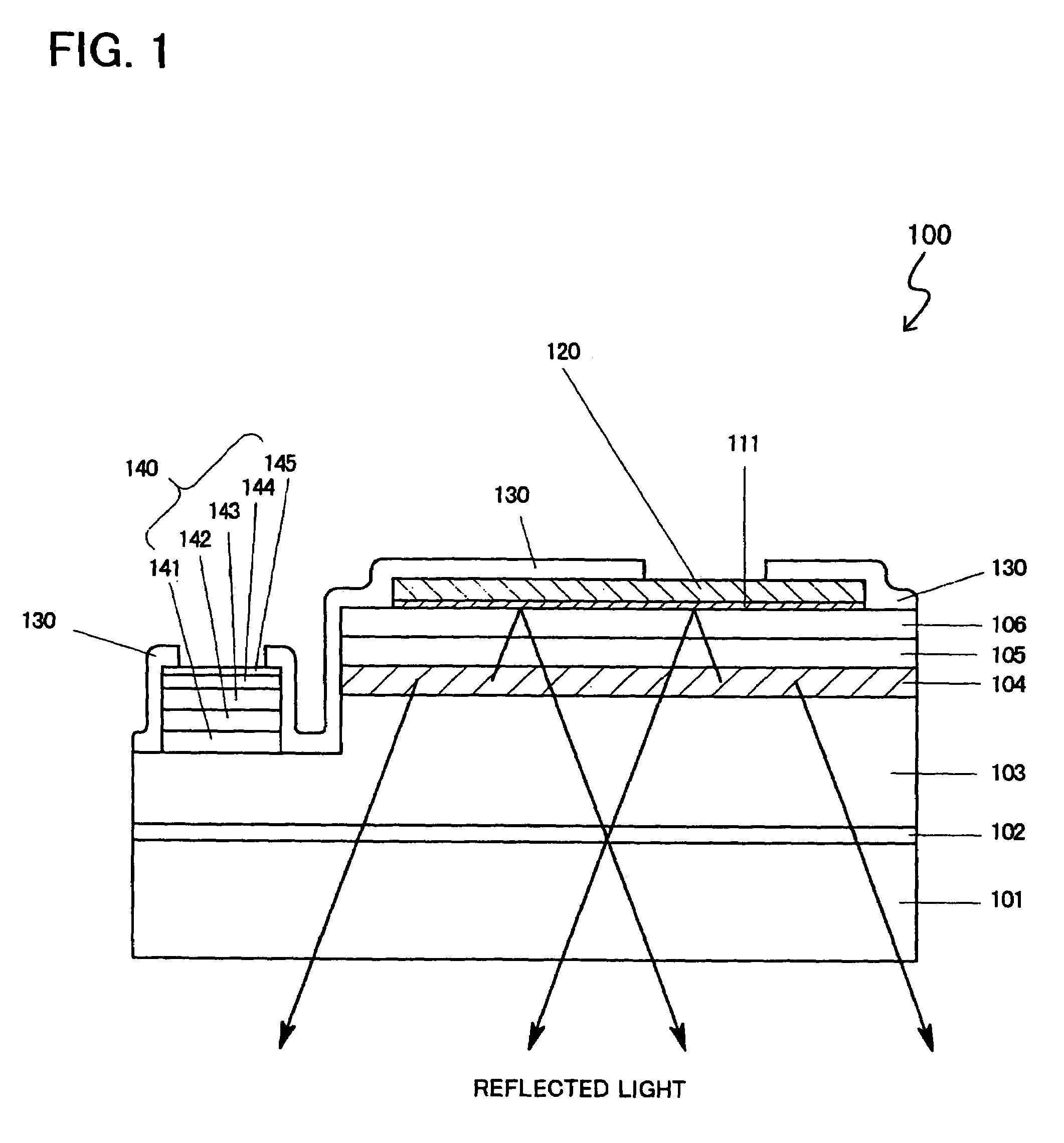
[0053]FIG. 1 illustrates a sectional view of a flip tip type of light-emitting semiconductor device 100. The semiconductor device 100 has a sapphire substrate 101 which has a buffer layer 102 made of nitride aluminum (AlN) having a thickness of 200 Å and an n+-layer 103 having a thickness of 4.0 μm with a high carrier concentration successively thereon.

[0054]And an emission layer 104 constructed with a multi quantum-well (MQW) structure made of GaN and Ga0.8In0.2N is formed on the n+-layer 103. A Mg-doped p-layer 105 made of Al0.15Ga0.85N having a thickness of 600 Å is formed on the emission layer 104. Further, a Mg-doped p-layer 106 made of GaN having a thickness of 1500 Å is formed on the p-layer 105.

[0055]A first thin-film metal layer 111 is formed by a metal deposit on the p-layer 106 and a negative electrode 140 is formed on the n+-layer 103. The first thin-film metal layer 111 is made at least one of of cobalt (Co) and nickel (Ni) having a thickness about 10 Å, and is adjacent...

second embodiment

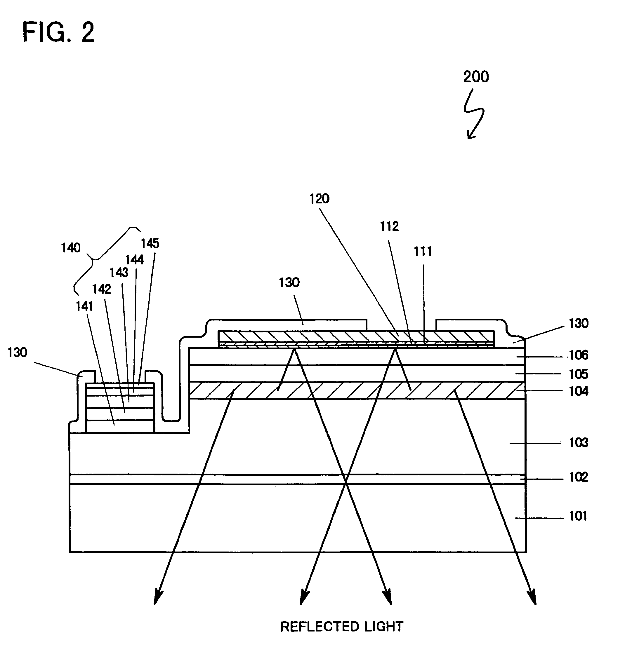
[0058]FIG. 2 shows a sectional view of a flip chip type of light-emitting semiconductor device 200 of the present invention. The semiconductor device 200 differs from the device 100 described in the first embodiment only in forming a second thin-film metal layer 112 on the first thin-film metal layer 111. The second thin-film metal layer 112 is made of Au having a thickness of about 150 Å, which is formed by a metal deposit after the first-thin film metal layer 111 is formed, in the same way of forming the first thin-film metal layer 111 made of cobalt (Go) or nickel (Ni) having a thickness of about 10 Å.

[0059]Forming this second thin-film metal layer 112 between the first thin-film metal layer 111 and the positive electrode (first positive electrode layer) 120 enables the positive electrode 120 to be connected to the layer 106 more firmly.

[0060]FIG. 3 shows a table to compare performances of each flip chip type of light-emitting semiconductor devices 100, 150, 200 and 400, respecti...

third embodiment

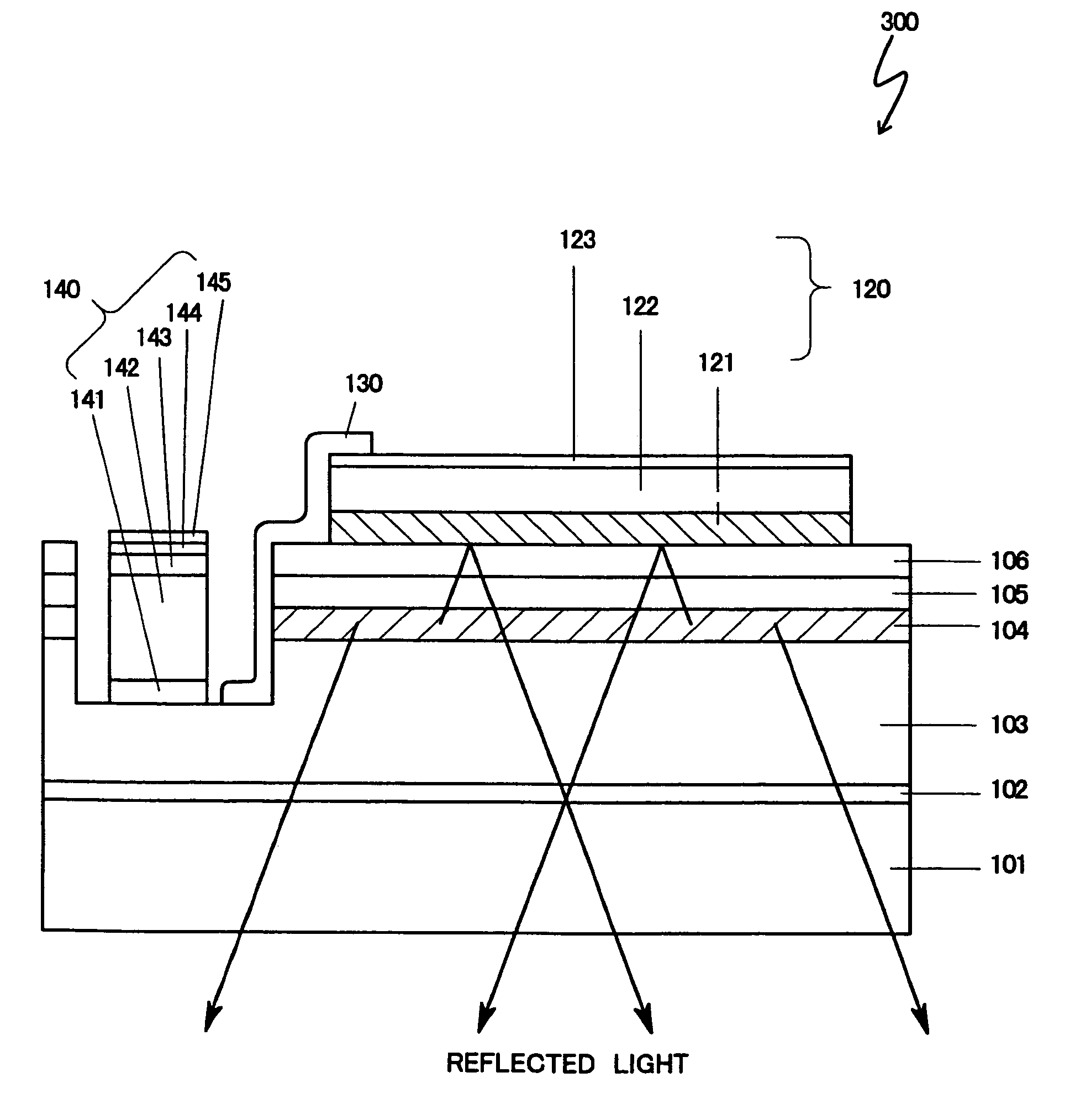
[0070]FIG. 4 illustrates a sectional view of a flip chip type of light-emitting semiconductor device 300. The semiconductor device 300 has a sapphire substrate 101 which has a buffer layer 102 made of nitride aluminum (AlN) having a thickness of 200 Å and an n+-layer 103 having a thickness of 4.0 μm and a high carrier concentration successively thereon.

[0071]And an emission layer 104 having a multi quantum-well (MQW) structure made of GaN and Ga0.8In0.2N is formed on the n+-layer 103. A Mg-doped p-layer 105 made of Al0.15Ga0.85N having a thickness of 600 Å is formed on the emission layer 104. Further, a Mg-doped p-layer 106 made of GaN having a thickness of 1500 Å is formed on the p-layer 105.

[0072]A positive electrode 120, which may be also referred to as a multiple positive electrode 120 hereinafter, is formed by a metal deposit on the p-layer 106 and a negative electrode 140 is formed on the n+-layer 103. The multiple positive electrode 120 is made of a three-layer structure, hav...


PUM

PropertyMeasurementUnit
wavelengthaaaaaaaaaa
thicknessaaaaaaaaaa
thicknessaaaaaaaaaa

Abstract

A flip chip type of light-emitting semiconductor device using group III nitride compound includes a thick positive electrode. The positive electrode, which is made of at least one of silver (Ag), rhodium (Rh), ruthenium (Ru), platinum (Pt) and palladium (Pd), and an alloy including at least one of these metals, is adjacent to a p-type semiconductor layer, and reflect light toward a sapphire substrate. Accordingly, a positive electrode having a high reflectivity and a low contact resistance can be obtained. A first thin-film metal layer, which is made of cobalt (Co) and nickel (Ni), or any combinations of including at least one of these metals, formed between the p-type semiconductor layer and the thick electrode, can improve an adhesion between an contact layer and the thick positive electrode. A thickness of the first thin-film metal electrode should be preferably in the range of 2 Å to 200 Å, more preferably 5 Å to 50 Å. A second thin-film metal layer made of gold (Au) can further improve the adhesion.

Description

[0001]The present Application is a Divisional Application of U.S. patent application Ser. No. 09 / 559,273, filed on Apr. 27, 2000 now U.S. Pat. No. 6,936,859, which was a Continuation Application of U.S. patent application Ser. No. 09 / 310,974, filed on May 13, 1999 now abandoned.BACKGROUND OF THE INVENTION[0002]1. Field of the Invention[0003]The present invention relates to a flip chip type of light-emitting semiconductor device that comprises layers using group III nitride formed on a sapphire substrate. Especially, the present invention relates to the device.[0004]2. Description of the Related Art FIG. 7 shows a sectional view of a conventional flip chip type of light-emitting semiconductor 400. Each 101, 102, 103, 104, 105, 106, 120, 130, and 140 represents a sapphire substrate, a buffer layer of AlN or GaN, an n-type GaN layer, an emission layer, a p-type AlGaN layer, a p-type GaN layer, a positive electrode, a protective film, a negative electrode having a multi-layer structure,...

Claims


Application Information

Patent Timeline
Patent Type & Authority Patents(United States)
IPC IPC(8): H01L29/22H01L31/072H01L33/32H01L33/40
CPCH01L33/405H01L33/32
Inventor UEMURA, TOSHIYAHORIUCHI, SHIGEMI
Owner TOYODA GOSEI CO LTD
Why Eureka
Try Eureka