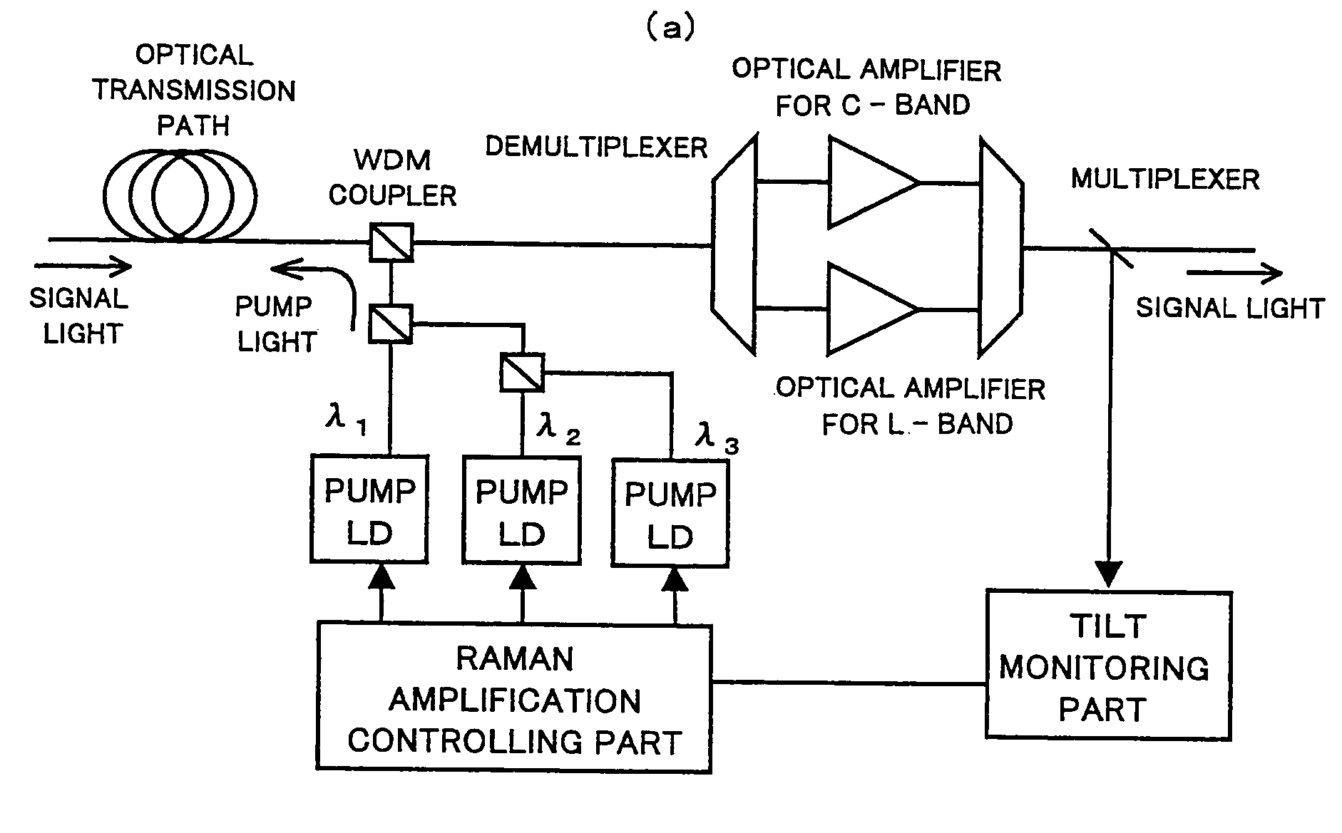
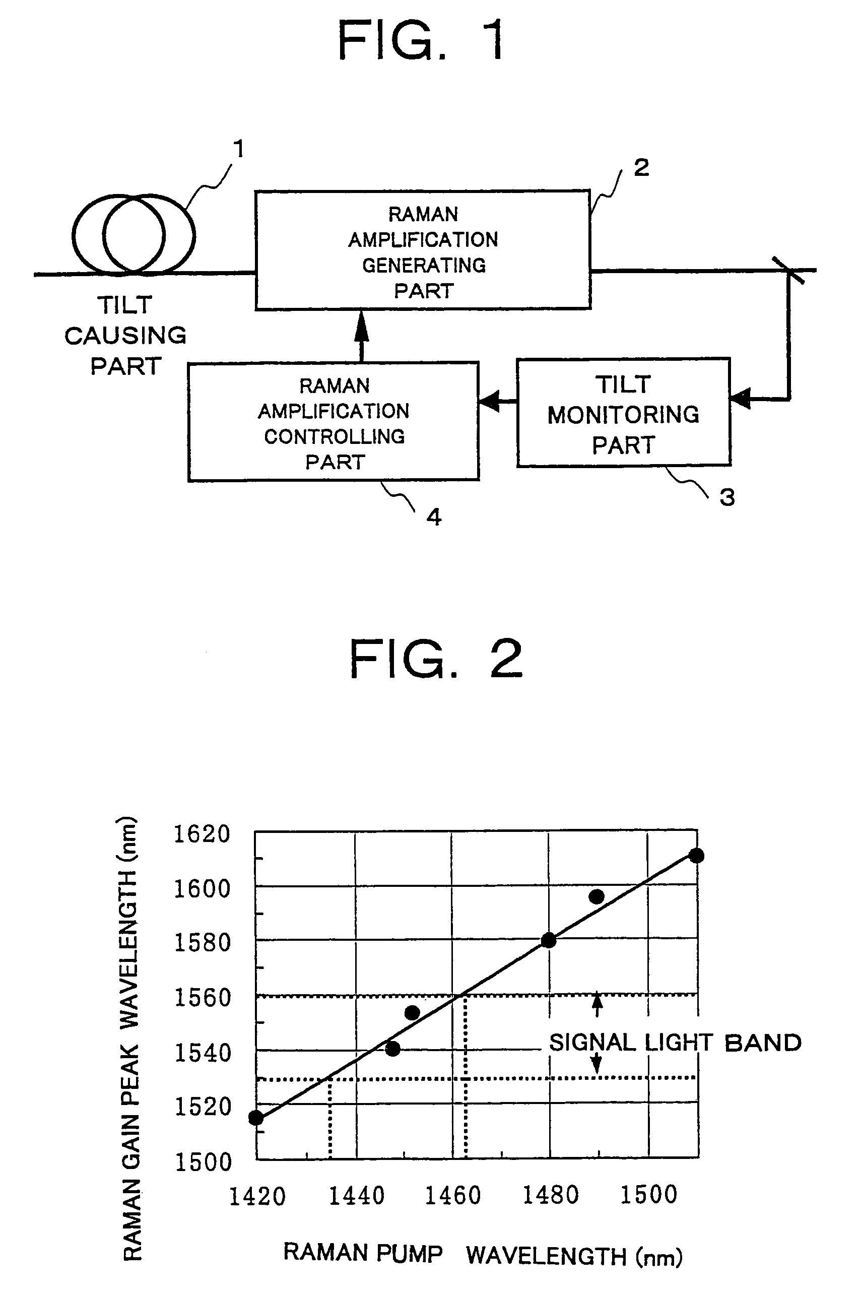
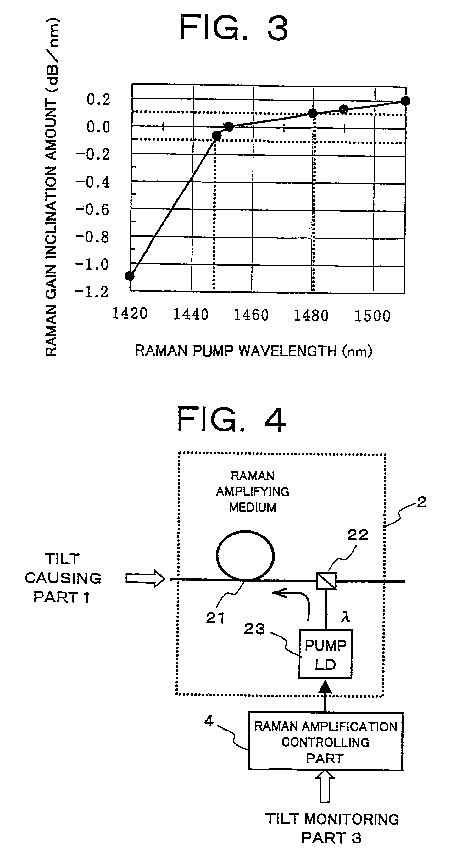
Raman pump power control for gain flattening

a technology of gain flattening and power control, which is applied in the direction of multiplex communication, electromagnetic repeaters, instruments, etc., can solve the problems of low limit, degraded optical s/n ratio, and thereby deteriorated transmission characteristics, and achieve the effect of improving transmission characteristics

Inactive Publication Date: 2006-09-19
FUJITSU LTD
View PDF13 Cites 17 Cited by
  • Summary
  • Abstract
  • Description
  • Claims
  • Application Information

AI Technical Summary

Benefits of technology

[0020]The present invention has been carried out in view of the points as described above, and it is therefore an object of the present invention to provide a method for controlling wavelength characteristics of optical transmission powers utilizing Raman amplification, in which wavelength characteristics of optical tra...

Problems solved by technology

This is because an upper limit of light power is restricted by nonlinear effect of a transmission path, and a lower limit thereof is restricted by a receiving S/N due to spontaneous emission light of an optical amplifier.
However, in the aforementioned conventional method for controlling wavelength characteristic of optical transmission powers, the optical transmission powers are equalized by giving losses to respective channels other than a channel having a minimum power in a manner match...

Method used


Image

  • Raman pump power control for gain flattening
  • Raman pump power control for gain flattening
  • Raman pump power control for gain flattening

Examples


first embodiment

[0142]FIG. 25 is a block diagram showing an entire constitution of a WDM optical communication system applied with the aforementioned basic constitution.

[0143]The system of FIG. 25 is applied with the aforementioned basic constitution by utilizing optical transmission paths 7 of respective repeater sections as Raman amplifying mediums, for a common WDM optical communication system which repeatingly transmits WDM signal light such as by interconnecting an optical sender (OS) 5 and an optical receiver (OR) 6 through the optical transmission paths 7 and by arranging optical amplifiers 8 on the way of the optical transmission paths 7, respectively.

[0144]Concretely, WDM couplers 22b are provided between output ends of optical transmission paths 7 and input ends of optical amplifiers 8 of repeater sections, respectively. Supplied from a backward side of each optical transmission path 7 via the WDM coupler 22b is pump light obtained by multiplexing by WDM couplers 22a pump light of 1,430 ...

second embodiment

[0160]There will be described hereinafter a

[0161]FIG. 28 is a block diagram showing an essential constitution of a WDM optical communication system according to the second embodiment of the present invention.

[0162]The system of FIG. 28 is applied with the aforementioned basic constitution by utilizing a dispersion compensation fiber (DCF) 9 as Raman amplification medium, for a WDM optical communication system in which wavelength dispersions caused in WDM signal light repeatingly transmitted through the optical transmission path 7 and optical amplifier 8 are compensated by the dispersion compensation fiber 9 inserted into a former stage of the optical receiver 6. Note, this type of system applied with the dispersion compensation fiber 9 as a part of transmission path is one which is being researched and developed for high-speed transmission of WDM signal light at 1.55 μm band making use of a transmission path comprising 1.3 μm zero-dispersion SMF. In the drawing, only the essential c...

third embodiment

[0170]There will be hereinafter described a

[0171]FIG. 31 is a block diagram showing a constitution of an optical amplifier according to a third embodiment applied with the aforementioned basic constitution.

[0172]The optical amplifier of FIG. 31 is applied with the aforementioned basic constitution by utilizing a dispersion compensation fiber (DCF) 84 as Raman amplification medium, for a known optical amplifier which includes a variable optical attenuator (VATT) 83 and the dispersion compensation fiber 84 both arranged between optical amplifying parts (EDFA) 81, 82 of two stage constitution.

[0173]Concretely, an input end of the former stage optical amplifying part 81 is connected to an input port IN of the present optical amplifier. Connected to an output end of the optical amplifying part 81 is an input end of latter stage optical amplifying part 82, via the variable optical attenuator 83 and dispersion compensation fiber 84. Connected to an output end of the optical amplifying part...


PUM


Abstract

The present invention aims at providing a method for controlling wavelength characteristics of optical transmission powers by Raman amplification, in which the wavelength characteristics of optical transmission powers are automatically compensated without giving any losses to channel lights to thereby improve transmission characteristics, and an apparatus adopting the same. To this end, the method for controlling wavelength characteristics of optical transmission powers by Raman amplification according to present invention supplies Raman pump light to an optical transmission path (Raman amplifying medium); compensates the wavelength characteristics of optical transmission powers caused by transmission of WDM signal light through the optical transmission path, by gain wavelength characteristics of generated Raman amplification; and monitors the wavelength characteristics of optical transmission powers after Raman amplification to thereby control the gain wavelength characteristics of Raman amplification.

Description

[0001]This application is a divisional of application Ser. No. 09 / 531,015, filed Mar. 20, 2000, now U.S. Pat. No. 6,785,042.BACKGROUND OF THE INVENTION[0002]1. Field of the Invention[0003]The present invention relates to a technique for controlling wavelength characteristics of optical transmission powers caused in wavelength division multiplexed signal light to be transmitted through an optical transmission path, and particularly to a method for compensating the wavelength characteristics of optical transmission powers making use of Raman amplification, as well as to a wavelength division multiplexing optical communication system and an optical amplifier to which the controlling method is applied.[0004]2. Related Art[0005]Wavelength division multiplexing (WDM) optical transmission system, such as making use of a wide gain band of an Erbium doped fiber amplifier, is capable of increasing a communication capacity by transmitting an optical signal including a plurality of wavelengths ...

Claims


Application Information

Patent Timeline
IPC IPC(8): H01S3/00H01S3/06G02F1/35H01S3/067H01S3/13H01S3/30H04B10/07H04B10/2519H04B10/2525H04B10/2537H04B10/29H04B10/296H04J14/00H04J14/02
CPCH04B10/296H01S3/1301H01S3/302H04B10/2916H04B10/294H04B10/2942H01S3/06758H01S3/06725H01S3/094011H01S3/094096H01S3/09415H01S3/10015H01S3/1305H01S2301/02H01S2301/04H01S3/13013
Inventor ONAKA, MIKIKINOSHITA, SUSUMU
Owner FUJITSU LTD
Why Eureka
Try Eureka