Method of fabricating SiGe Bi-CMOS device

a bi-cmos and semiconductor technology, applied in the direction of semiconductor devices, basic electric elements, electrical equipment, etc., can solve the problems of difficult realization of nano-scale ultra-high speed and ultra-low power devices, and achieve the effect of preventing an abrupt increase of contact resistance and improving the radio frequency (rf) characteristic of heterojunction bipolar transistors

Inactive Publication Date: 2006-10-03
ELECTRONICS & TELECOMM RES INST
View PDF9 Cites 15 Cited by
  • Summary
  • Abstract
  • Description
  • Claims
  • Application Information

AI Technical Summary

Benefits of technology

[0008]The present invention is directed to implementation of a method of fabricating a silicon germanium (SiGe) Bi-CMOS device, in which a silicide process using nickel (Ni) is employed, thereby improving a radio frequency (RF) characteristic of a heterojunction bipolar transistor (HBT), and preventing an abrupt increase of contact resistance due to a reduction in linewidth of a CMOS device.

Problems solved by technology

However, in the case where a device has a linewidth less than 100 nm and is fabricated using a conventional method, the resistance abruptly increases, thereby making it difficult to realize a nano-scale ultra-high speed and ultra-low power device.

Method used


Image

  • Method of fabricating SiGe Bi-CMOS device
  • Method of fabricating SiGe Bi-CMOS device
  • Method of fabricating SiGe Bi-CMOS device

Examples


Embodiment Construction

[0018]Hereinafter, an exemplary embodiment of the present invention will be described in detail. However, the present invention is not limited to the embodiments disclosed below, but can be implemented in various types. Therefore, the present embodiment is provided for complete disclosure of the present invention and to fully inform the scope of the present invention to those ordinarily skilled in the art.

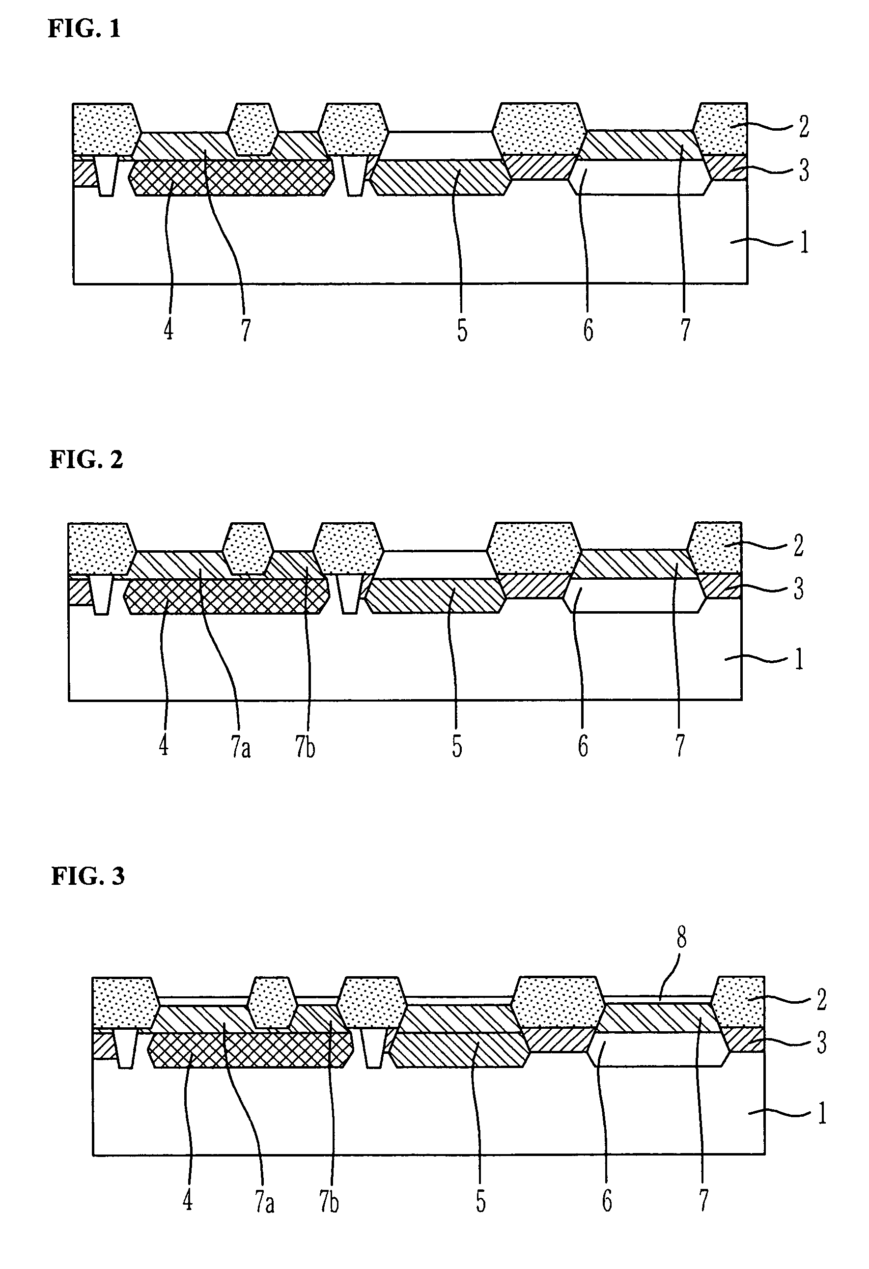
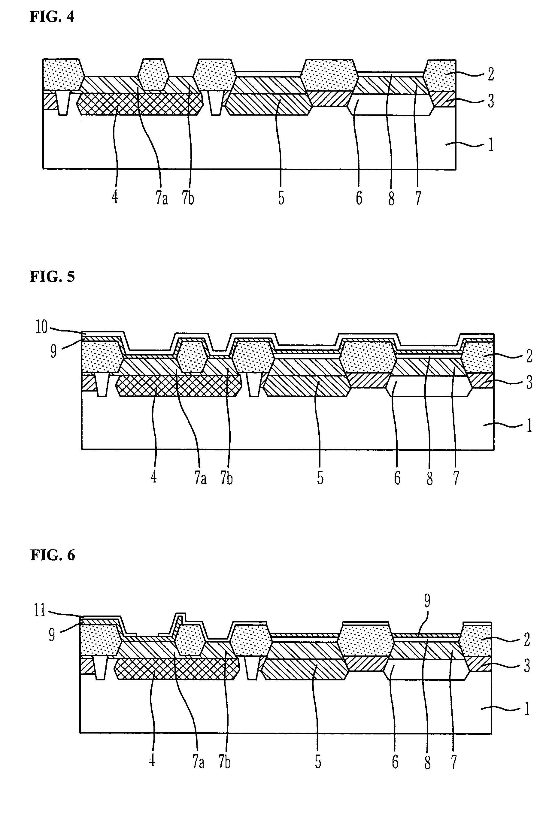
[0019]FIGS. 1 to 15 are cross-sectional views illustrating a method of fabricating a silicon germanium (SiGe) Bi-CMOS device according to an exemplary embodiment of the present invention.

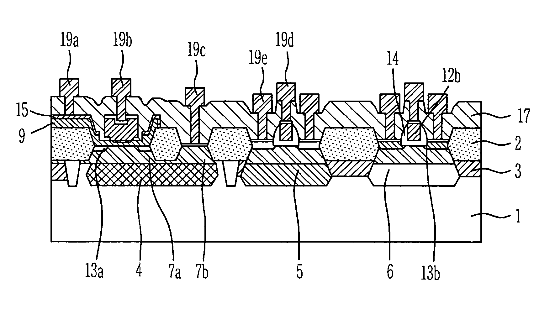
[0020]Referring to FIG. 1, an isolation junction region 3 and an isolation layer 2 are formed on a semiconductor substrate 1 to define a silicon germanium (SiGe) heterojunction bipolar transistor (HBT) region, an NMOS transistor (NMOS) region, and a PMOS transistor (PMOS) region. An N+ sub-collector region 4 is formed in the substrate 1 of the HBT region, a P-well region 5 is formed in the substrat...


PUM


Abstract

Provided is a method of fabricating a silicon germanium (SiGe) Bi-CMOS device. In the fabrication method, the source and drain of the CMOS device is formed using a silicon germanium (SiGe) heterojunction, instead of silicon, thereby preventing a leakage current resulting from a parasitic bipolar operation. Further, since the source and drain is connected with an external interconnection through the nickel (Ni) silicide layer, the contact resistance is reduced, thereby preventing loss of a necessary voltage for a device operation and accordingly, making it possible to enable a low voltage and low power operation and securing a broad operation region even in a low voltage operation of an analogue circuit.

Description

CROSS-REFERENCE TO RELATED APPLICATION[0001]This application claims priority to and the benefit of Korean Patent Application No. 2004-100826, filed Dec. 3, 2004, the disclosure of which is incorporated herein by reference in its entirety.BACKGROUND[0002]1. Field of the Invention[0003]The present invention relates to a method of fabricating a semiconductor device, and more particularly, to a method of fabricating a silicon germanium (SiGe) Bi-CMOS device having a CMOS transistor and a SiGe heterojunction bipolar transistor (HBT) using an epitaxial layer containing germanium (Ge) as a base.[0004]2. Discussion of Related Art[0005]SiGe Bi-CMOS technology has been recognized as the most suitable technology for fabricating a System on Chip (SoC) of radio frequency (RF) / analogue / digital among various wireless mobile communication components. In a modern wireless mobile communication field having a mainstream of miniaturization and multifunction, the SiGe Bi-CMOS technology is widely used i...

Claims


Application Information

Patent Timeline
Patent Type & Authority Patents(United States)
IPC IPC(8): H01L21/8238
CPCH01L21/8249H01L27/06
Inventor BAE, HYUN CHEOLLEE, SEUNG YUNKIM, SANG HUNKANG, JIN YEONG
Owner ELECTRONICS & TELECOMM RES INST
Why Eureka
Try Eureka