

Systems and method for forming silicon oxide layers
a silicon oxide and layer technology, applied in the direction of coatings, capacitors, chemical vapor deposition coatings, etc., can solve the problems of reducing the effect of the layer as an insulator, reducing the efficiency of the layer, so as to reduce the detrimental gas phase reaction and improve the control of the thickness of the layer
Inactive Publication Date: 2006-10-03
MICRON TECH INC
View PDF68 Cites 161 Cited by
- Summary
- Abstract
- Description
- Claims
- Application Information
AI Technical Summary
Benefits of technology
The present invention provides methods for depositing metal oxide and silicon oxide layers on a substrate using vapor deposition processes with ozone. These methods do not require the use of water or other hydrogen-producing coreactants, reducing the problem of producing hydrogen-containing layers. The methods involve contacting a substrate with precursor compounds of the formula M(NR1R2)x(NR3)y or Si(NR1R2)xZy, wherein M or R2 are each independently hydrogen or an organic group, and Z is Cl or H. The methods can be used to form metal oxide or silicon oxide layers on a variety of substrates, such as semiconductor devices. The methods provide a way to deposit layers with high precision and purity, and can be used in the manufacturing of memory device structures.
Problems solved by technology
The continuous shrinkage of microelectronic devices such as capacitors and gates over the years has led to a situation where the materials traditionally used in integrated circuit technology are approaching their performance limits.
However, when the SiO2 layer is thinned to 1 nm (i.e., a thickness of only 4 or 5 molecules), as is desired in the newest micro devices, the layer no longer effectively performs as an insulator due to the tunneling current running through it.
However, undesirable chlorine residues can also be formed.
They would also likely leave carbon in the resultant films.
Method used
View moreImage
Smart ImageViewing Examples

Examples
example
Example 1
Atomic Layer Deposition of HfO2
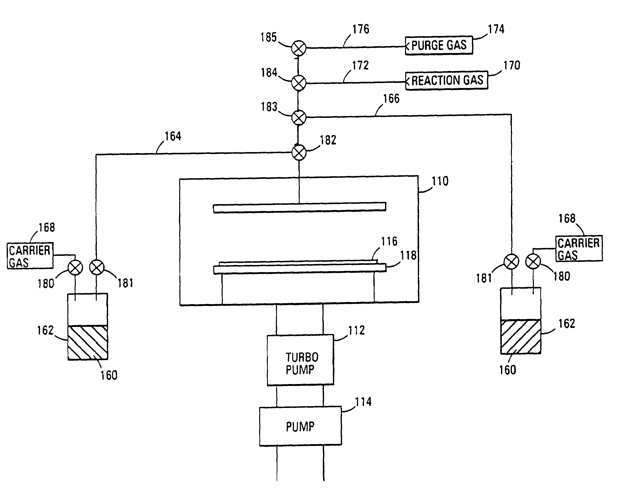
[0093]Using an ALD process, precursor compounds hafnium dimethylamide, Hf(N(CH3)2)4 (Strem Chemicals, Newbury Port, Mass.), and an ozone / oxygen (O3 / O2) mixture, having approximately 10% ozone by weight, were alternately pulsed for 600 cycles into a deposition chamber containing a BPSG substrate. A 590 Å layer of HfO2 was deposited, containing 37 atom % Hf, and 63 atom % oxygen. The layer of HfO2 was, surprisingly, free of carbon and nitrogen within detection limits of XPS at a substrate temperature of approximately 220° C.
Login to View More PUM
| Property | Measurement | Unit |
|---|---|---|
| temperature | aaaaa | aaaaa |
| thickness | aaaaa | aaaaa |
| adsorption energies | aaaaa | aaaaa |
Abstract
A method of forming (and apparatus for forming) a metal oxide layer, preferably a dielectric layer, on a substrate, particularly a semiconductor substrate or substrate assembly, using a vapor deposition process and ozone with one or more metal organo-amine precursor compounds.
Description
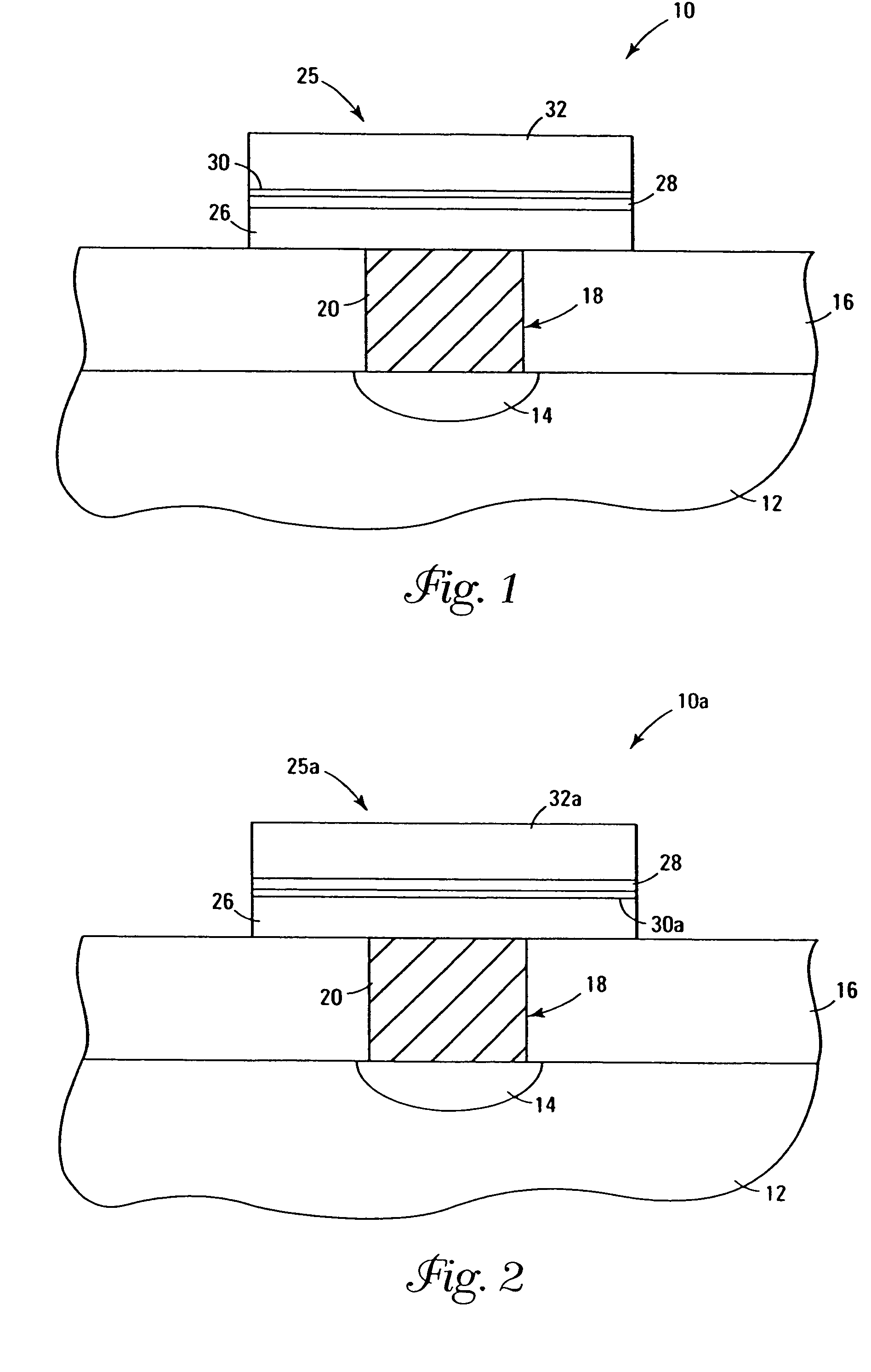
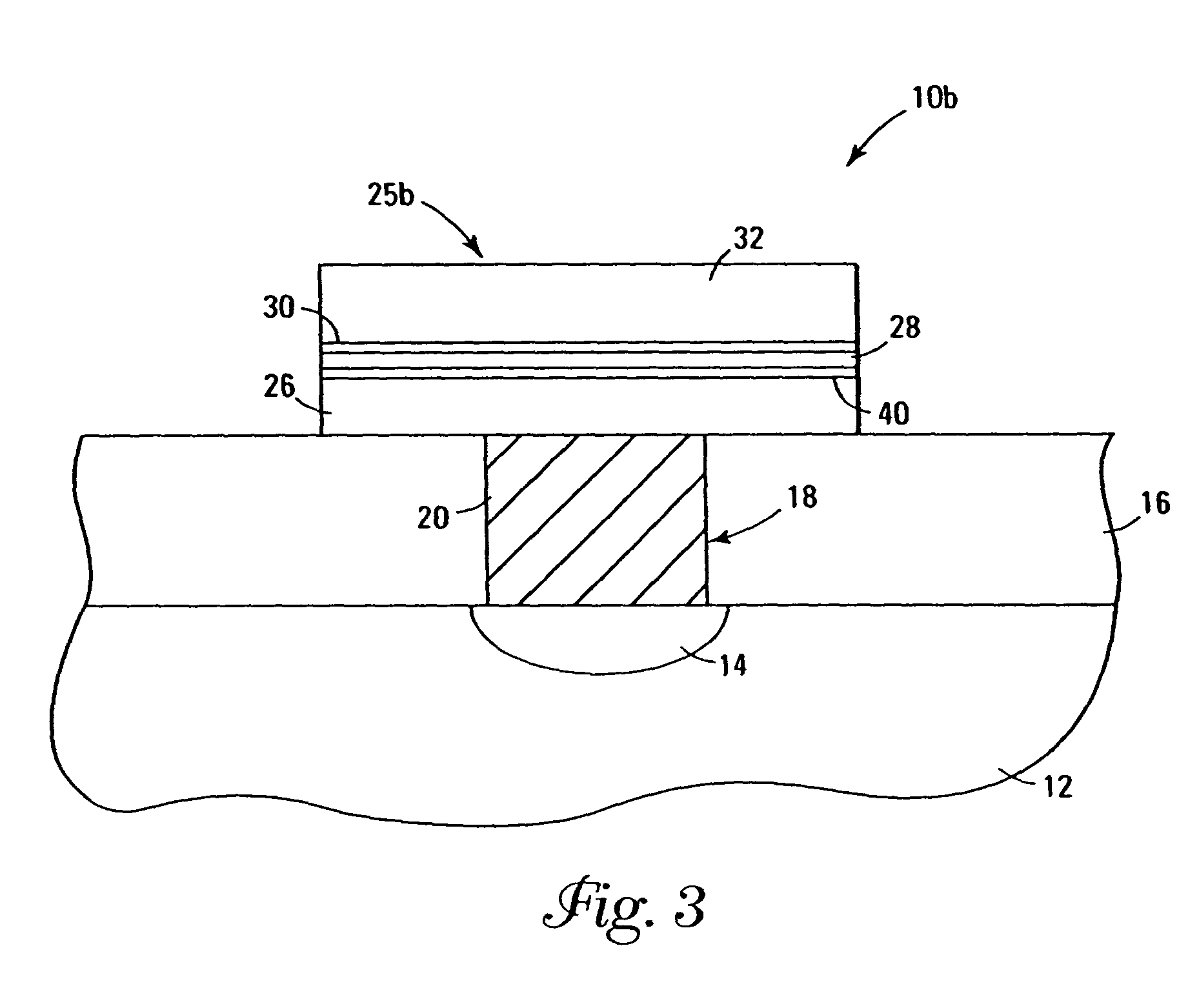
FIELD OF THE INVENTION[0001]This invention relates to methods of forming a layer on a substrate using one or more metal precursor compounds and ozone during a vapor deposition process. The precursor compounds and methods are particularly suitable for the formation of a metal oxide layer, particularly a metal oxide dielectric layer, onto a semiconductor substrate or substrate assembly.BACKGROUND OF THE INVENTION[0002]Capacitors are the basic energy storage devices in random access memory devices, such as dynamic random access memory (DRAM) devices and static random access memory (SRAM) devices. They consist of two conductors, such as parallel metal or polysilicon plates, which act as the electrodes (i.e., the storage node electrode and the cell plate capacitor electrode), insulated from each other by a dielectric material.[0003]The continuous shrinkage of microelectronic devices such as capacitors and gates over the years has led to a situation where the materials traditionally used ...
Claims
Login to View More Application Information
Patent Timeline
 Patent Type & AuthorityPatents(United States)
IPC IPC(8): H01L21/31C23C16/40C23C16/455H01L21/314H01L21/316
CPCC23C16/40C23C16/401C23C16/45553H01L21/02164H01L21/02181H01L21/02219H01L21/0228H01L21/3141H01L21/31612H01L21/31645H01L28/40H01L21/31616H01L21/02271H01L21/02186
InventorVAARTSTRA, BRIAN A.QUICK, TIMOTHY A.
OwnerMICRON TECH INC