Low power charge pump

a technology of low power consumption and charge pump, which is applied in the direction of power conversion system, dc-dc conversion, instruments, etc., can solve the problems of inefficiency of power conversion circuits implemented on integrated circuits, process steps, and potentially very dense silicon-oxide-nitride-oxide-silicon (sonos) that cannot be fully charged, so as to increase the efficiency of charge pump. , the effect of high efficiency

Inactive Publication Date: 2006-10-03
INFINEON TECH LLC
View PDF8 Cites 53 Cited by
  • Summary
  • Abstract
  • Description
  • Claims
  • Application Information

AI Technical Summary

Benefits of technology

[0024]Embodiments of the present invention provide a means to increase the efficiency of charge pumps. Further embodiments of the present invention provide for increasing the efficiency of charge pumps in a manner that is compatible and complimentary with conventional approaches to implementing high efficiency charge pumps. Still further embodiments of the present invention provide for the above mentioned solutions to be achieved with existing semiconductor processes and equipment without revamping well established tools and techniques.
[0025]A low power charge pump is disclosed. A pump driving node of a first pump stage is selectively coupled to a pump driving node of the subsequent pump stage. Subsequent to a transfer of charge from a first pump stage to a subsequent stage, the first and subsequent pump driving nodes are coupled. Residual charge on a first stage pump driving node is thereby transferred to a subsequent pump driving node. Subsequent to the transfer of charge from the first pump driving node to the second pump driving node, the nodes are uncoupled. By selectively coupling a first pump stage to a pump driving node of the subsequent pump stage, the first pump driving node may pre-charge the subsequent pump driving node, thereby reducing the energy that must be provided by clock driving circuitry to produce a positive-going transition of a driving clock. Advantageously, pre-charging energy is taken from the first stage, reducing the energy that was heretofore dissipated by clock driving circuitry during a negative-going clock signal transition.

Problems solved by technology

Silicon-Oxide-Nitride-Oxide-Silicon (SONOS) is potentially very dense in terms of number of cells per unit area that can be used and it requires fewer process steps as compared to floating gate memory.
Memory device manufacturers are continually challenged to provide ever greater amounts of memory at ever lower costs.
Unfortunately, power conversion circuits implemented on an integrated circuit are typically less efficient at converting energy from one voltage to another than a system-level circuit board implementation of a voltage conversion circuit.
Among the factors contributing to lower efficiencies is the general commercial unfeasibility of rendering an inductor of sufficient value for use in a power conversion circuit.
Semiconductor processing equipment is extremely expensive.
Fundamental semiconductor processing steps, e.g., implantation and diffusion, typically require long periods of development and extensive qualification testing.
Implementing a new fabrication process requires considerable resources on the part of the semiconductor manufacturer.
Additionally, re-tooling a fabrication line is very expensive, both in terms of direct expenses as well as in terms of opportunity cost due to the time required to perform the re-tooling.

Method used


Image

  • Low power charge pump
  • Low power charge pump
  • Low power charge pump

Examples


Embodiment Construction

[0036]In the following detailed description of the present invention, low power charge pump, numerous specific details are set forth in order to provide a thorough understanding of the present invention. However, it will be recognized by one skilled in the art that the present invention may be practiced without these specific details or with equivalents thereof. In other instances, well-known methods, procedures, components, and circuits have not been described in detail so as not to unnecessarily obscure aspects of the present invention.

Low Power Charge Pump

[0037]Embodiments of the present invention are described in the context of design and operation of flash memory devices. However, it is appreciated that embodiments of the present invention may be utilized in other areas of electronic design and operation.

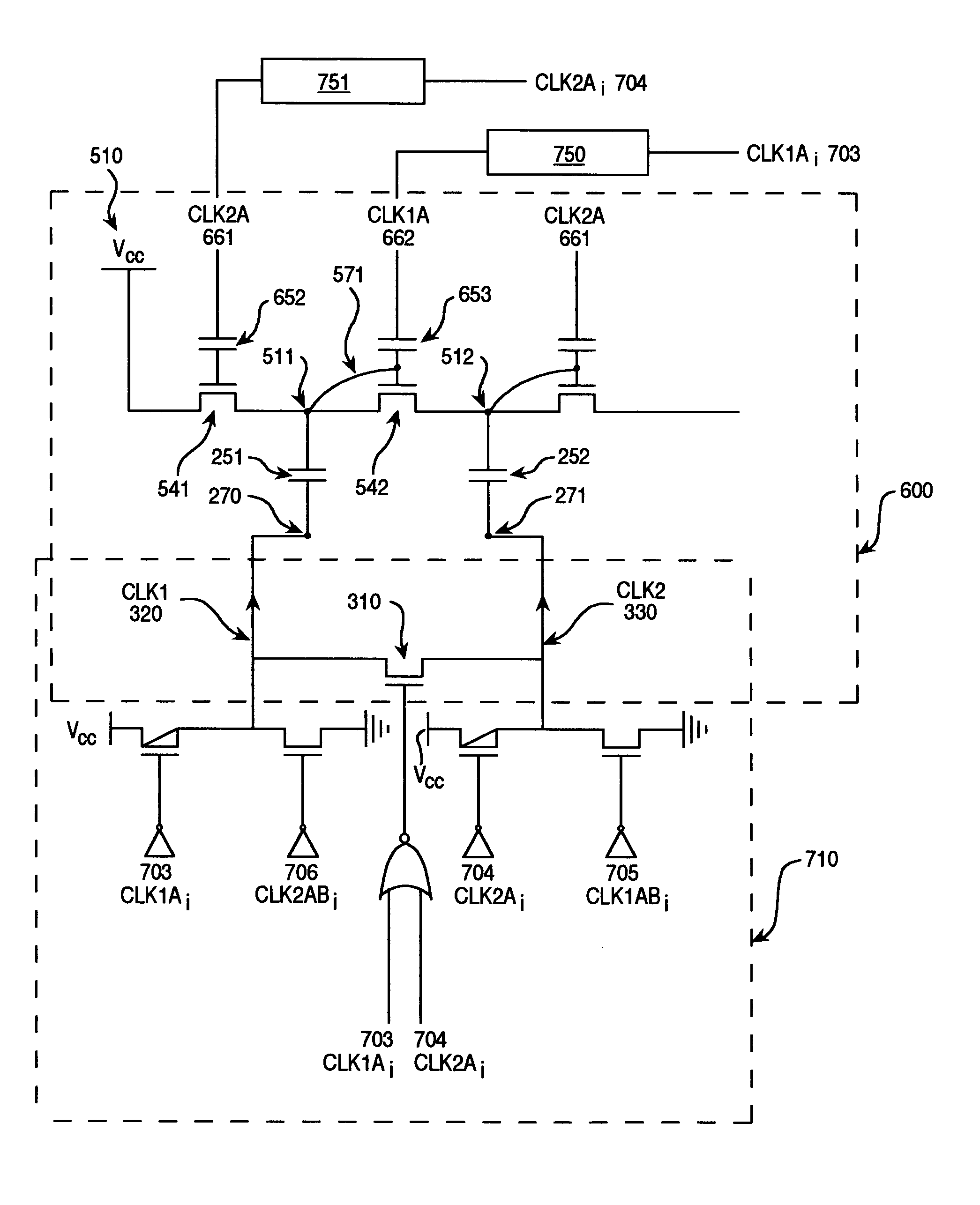
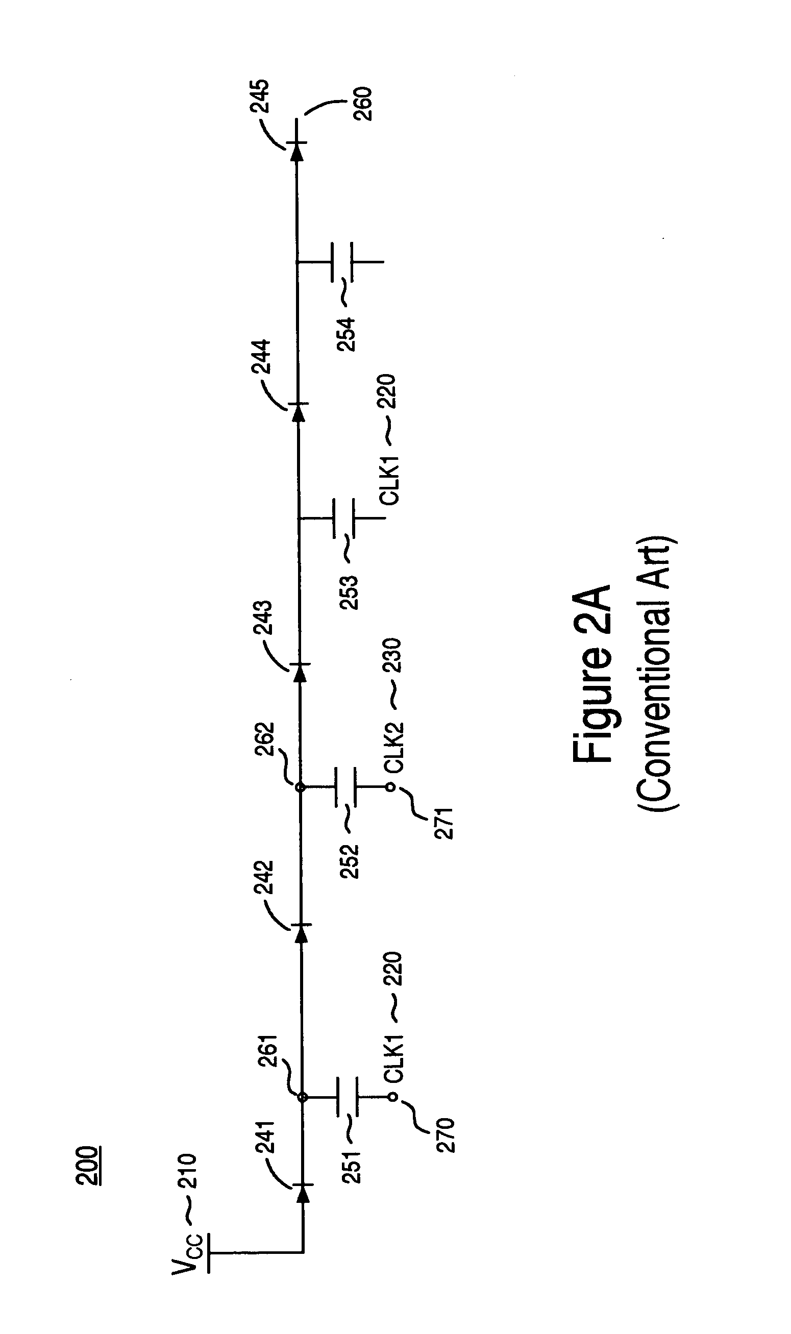
[0038]Referring once again to FIGS. 2A and 2B, a negative clock transition at the bottom terminal of the capacitive elements, e.g., at pump driving node 270, is a functional el...


PUM


Abstract

A low power charge pump is disclosed. A pump driving node of a first pump stage is selectively coupled to a pump driving node of the subsequent pump stage. Subsequent to a transfer of charge from a first pump stage to a subsequent stage, the first and subsequent pump driving nodes are coupled. Residual charge on a first stage pump driving node is thereby transferred to a subsequent pump driving node. Subsequent to the transfer of charge from the first pump driving node to the second pump driving node, the nodes are uncoupled. By selectively coupling a first pump stage to a pump driving node of the subsequent pump stage, the first pump driving node may pre-charge the subsequent pump driving node, thereby reducing the energy that must be provided by clock driving circuitry to produce a positive-going transition of a driving clock. Advantageously, pre-charging energy is taken from the first stage, reducing the energy that was heretofore dissipated by clock driving circuitry during a negative-going clock signal transition. In this novel manner conversion efficiency of a charge pump device may be beneficially increased, providing enhanced low power performance.

Description

TECHNICAL FIELD[0001]Embodiments of the present invention relate to design and operation of sub-micron metal oxide semiconductors. More particularly, embodiments of the present invention provide a low power charge pump.BACKGROUND ART[0002]Flash memory is a type of semiconductor computer memory with many desirable characteristics. Like read only memory, ROM, it is non-volatile, meaning that the contents of the memory are stable and retained without applied electrical power.[0003]Flash memory devices have found wide commercial success in the electronic device market. A major advantage of flash over ROM is that the memory contents of flash may be changed after the device is manufactured. Flash memory has found wide acceptance in many types of computers, including desktop computers, mobile phones and hand held computers. Flash memory is also widely used in digital cameras and portable digital music players, for example “MP3” players.[0004]In addition to direct flash storage applications...

Claims


Application Information

Patent Timeline
Patent Type & Authority Patents(United States)
IPC IPC(8): G05F3/24H02M3/07
CPCH02M3/073G11C5/145G11C16/30H02M3/07G11C16/0408
Inventor GUO, XIN
Owner INFINEON TECH LLC
Why Eureka
Try Eureka