Electrochemical test sensor
- Summary
- Abstract
- Description
- Claims
- Application Information
AI Technical Summary
Benefits of technology
Problems solved by technology
Method used
Image
Examples
example i
Metal Converted to Metal Oxide / Metal Halide Construction
[0022]The sensor is constructed using various layers of polymer thick film (PTF) to form the working sensor. The conductive leads and trigger subunit is printed from any standard conductive PTF utilizing a metal pigment for high conductivity. In this case, a thermoplastic silver / graphite PTF was used for its cost advantage and cured in an air furnace. The working and counter electrodes were printed using a standard carbon / graphite PTF and the area can be defined using a standard UV or conventional dielectric PTF. The curing of the PTF converts the silver to silver oxide on the PTF surface. Any remaining silver on the surface of the trigger sub-electrode is further converted using an oxygen plasma process that is currently used to improve the performance of the working electrode surface as disclosed in U.S. Pat. No. 5,429,735. This plasma process could also use a halide gas that can react with the metal to form a metal halide at...
example ii
Metal Oxide Construction
[0023]The sensor can be constructed using various layers of PTF's where the trigger PTF has incorporated in it a metal oxide or metal halide. The advantage of this system is that it does not need to be converted to form the necessary electropositive material. In this example, a specialty PTF ink is made using AgO and graphite to form the conductive leads. This ink is screen printed as previously described except that the AgO is not formed during the subsequent air curing or O2 plasma treatment. The electrode and dielectric PTF is printed and cured as in Example I.
[0024]Other metal oxides can be used in the manufacture of the PTF, but depending on the conductivity of the oxide it may not function as well for the conducting leads, so that a separate print from the conductive leads would be required. This would increase the cost of manufacturing the sensor due to the need for an additional printing layer.
example iii
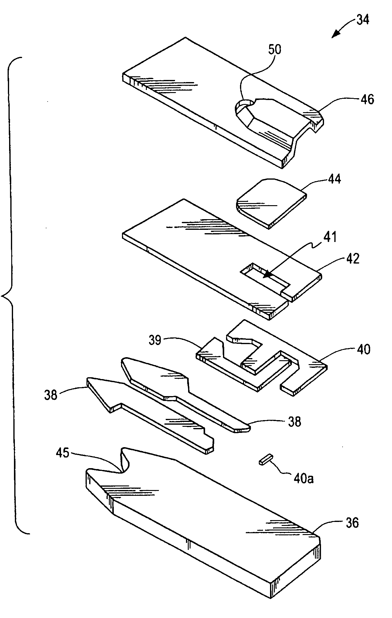
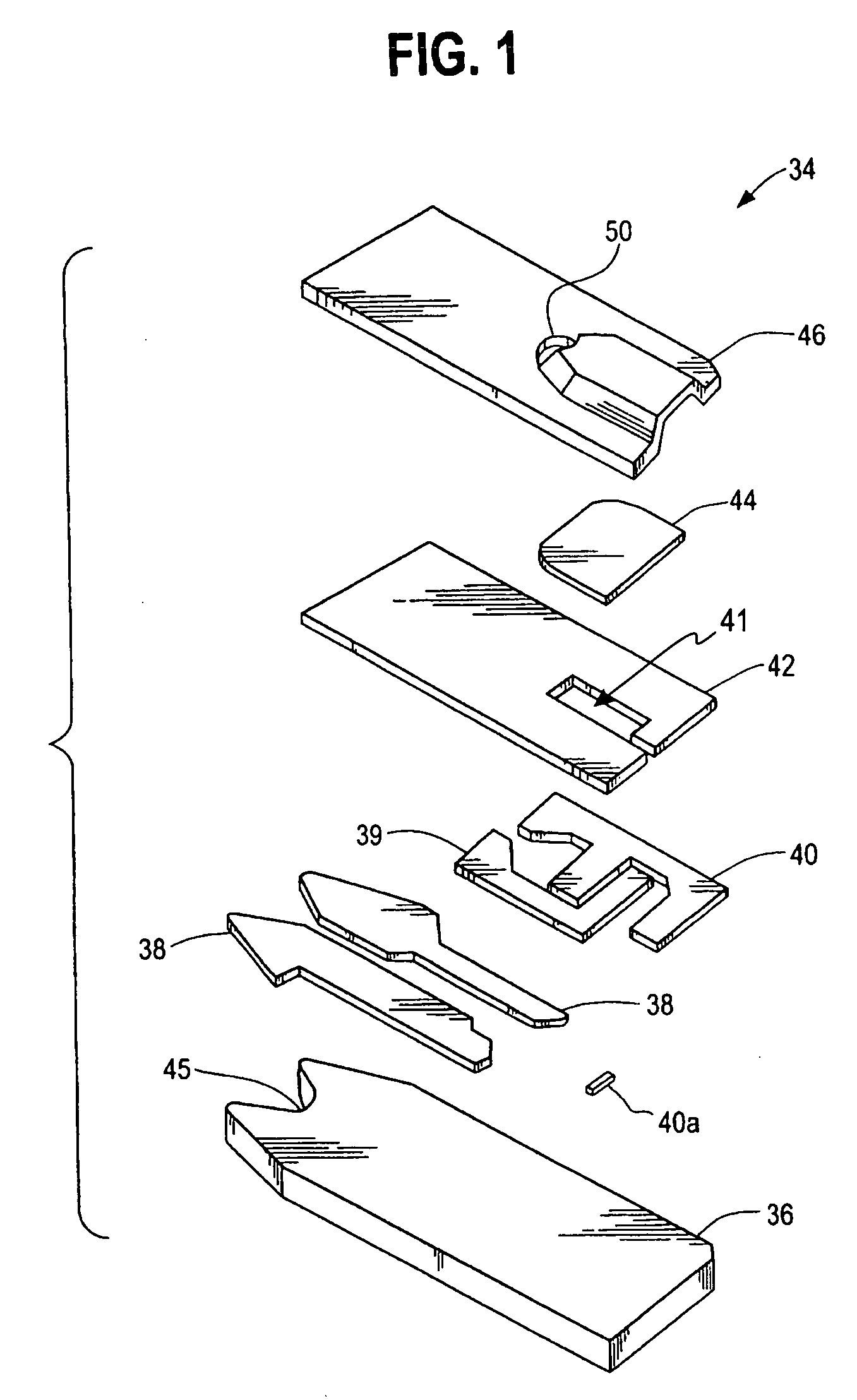
[0025]A base stock, typically of polycarbonate, is printed with various inks to form the electrodes 39 and 40 and then overcoated with a dielectric layer 42 in a predetermined pattern designed to leave a desired surface of the electrode exposed to contact by the fluid test sample as it enters the space formed by mating the lid 46 and the base 36. The particular configuration of the dielectric layer 42 is as depicted in FIG. 1 in which opening 43 leaves the reagent layer in electrical communication with the electrodes 39 and 40 is designed to define the extent to which all of the conductive elements (working, reference and sub-element electrodes) are exposed to the test fluid. Along with the printed conductive features, the dielectric layer defines the size of each of these elements. The electrodes are preferably printed so that the conductive and dielectric layers are close to 90 degrees to each other. This helps in the tolerance stackup for building the sensor because it reduces th...
PUM
| Property | Measurement | Unit |
|---|---|---|
| thick | aaaaa | aaaaa |
| volume | aaaaa | aaaaa |
| volume | aaaaa | aaaaa |
Abstract
Description
Claims
Application Information


