Ion-assisted oxidation methods and the resulting structures

a technology of ion-assisted oxidation and ion-assisted oxidation, which is applied in the direction of basic electric elements, electrical equipment, semiconductor devices, etc., can solve the problems of increasing the gate-induced drain leakage, degrading the gate dielectric intensity, and partially etching the gate dielectric, so as to reduce the warpage of the wafer, reduce the thermal stress, and reduce the effect of crystal defects

Inactive Publication Date: 2006-10-10
MICRON TECH INC
View PDF57 Cites 4 Cited by
  • Summary
  • Abstract
  • Description
  • Claims
  • Application Information

AI Technical Summary

Benefits of technology

[0008]The present invention permits a high-quality thin oxide layer to be formed at relatively low temperatures when compared with conventional techniques. Low-temperature oxidation leads to fewer thermal stresses, fewer crystal defects, less wafer warpage, and reduction of oxidation-enhanced diffusion. The present invention also allows less oxidation of the sidewalls of conductive layers in transistor gate structures to occur during oxidation. The present invention also facilitates fabrication of a transistor exhibiting lower amounts of current leakage to source and drain regions during operation.

Problems solved by technology

Unfortunately, the gate dielectric will be etched partially during the dry etch of the gate conductor.
A thinner gate dielectric along the gate conductor edge will degrade the gate dielectric intensity and increase the gate-induced drain leakage.
High-temperature oxidation, however, can cause problems such as changes in impurity profiles, non-uniform oxide thicknesses along the side wall of the gate conductor, and defect formation in the underlying substrate.
When certain metals, such as tungsten, are used as the gate conductor, a high-temperature oxidation process can form materials, such as tungsten oxide, that are volatile and can cause product yield loss.
Most of these low-temperature techniques, however, fail to produce the high-quality gate dielectric necessary to maintain good gate dielectric integrity and low leakage.

Method used


Image

  • Ion-assisted oxidation methods and the resulting structures
  • Ion-assisted oxidation methods and the resulting structures
  • Ion-assisted oxidation methods and the resulting structures

Examples


Embodiment Construction

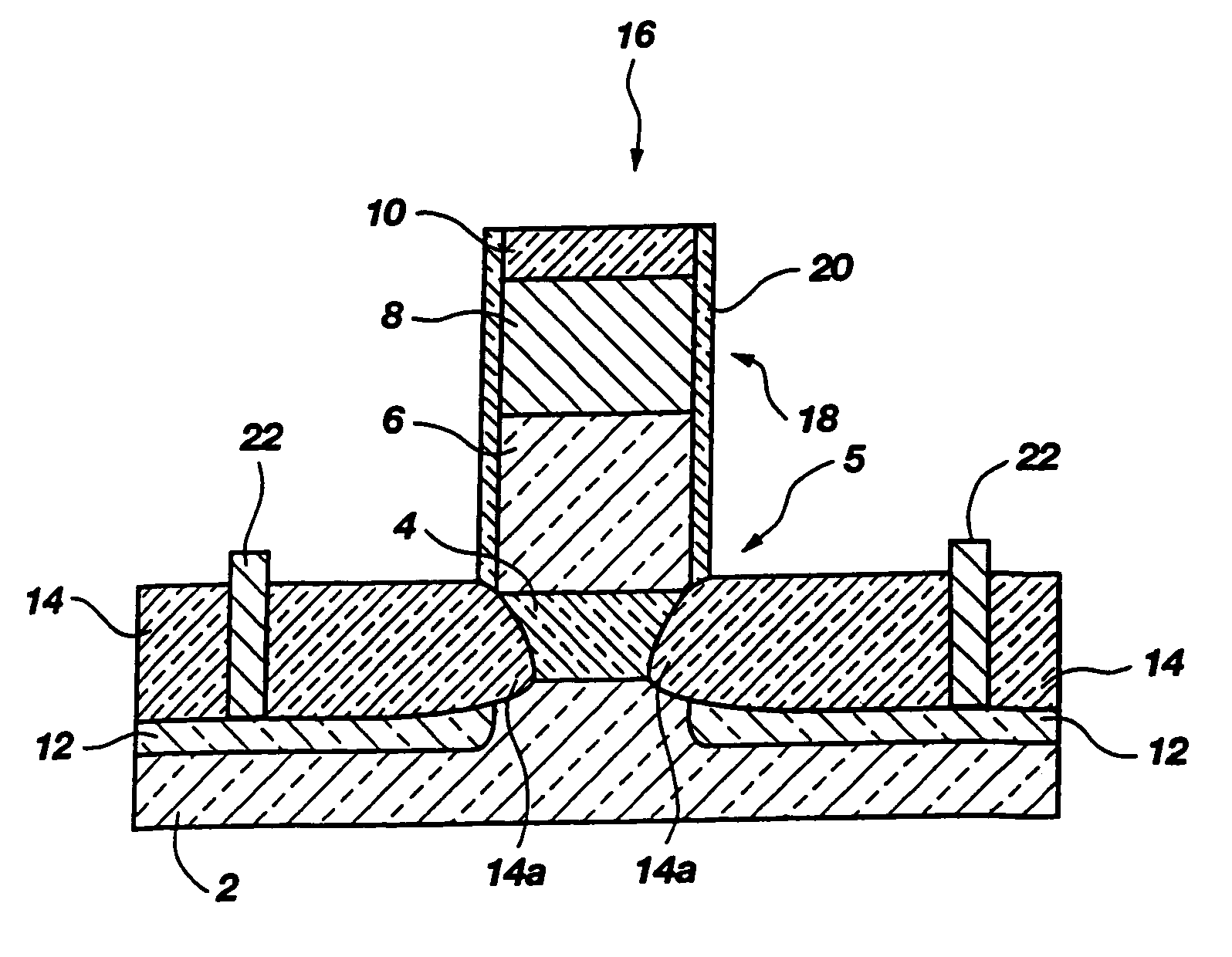
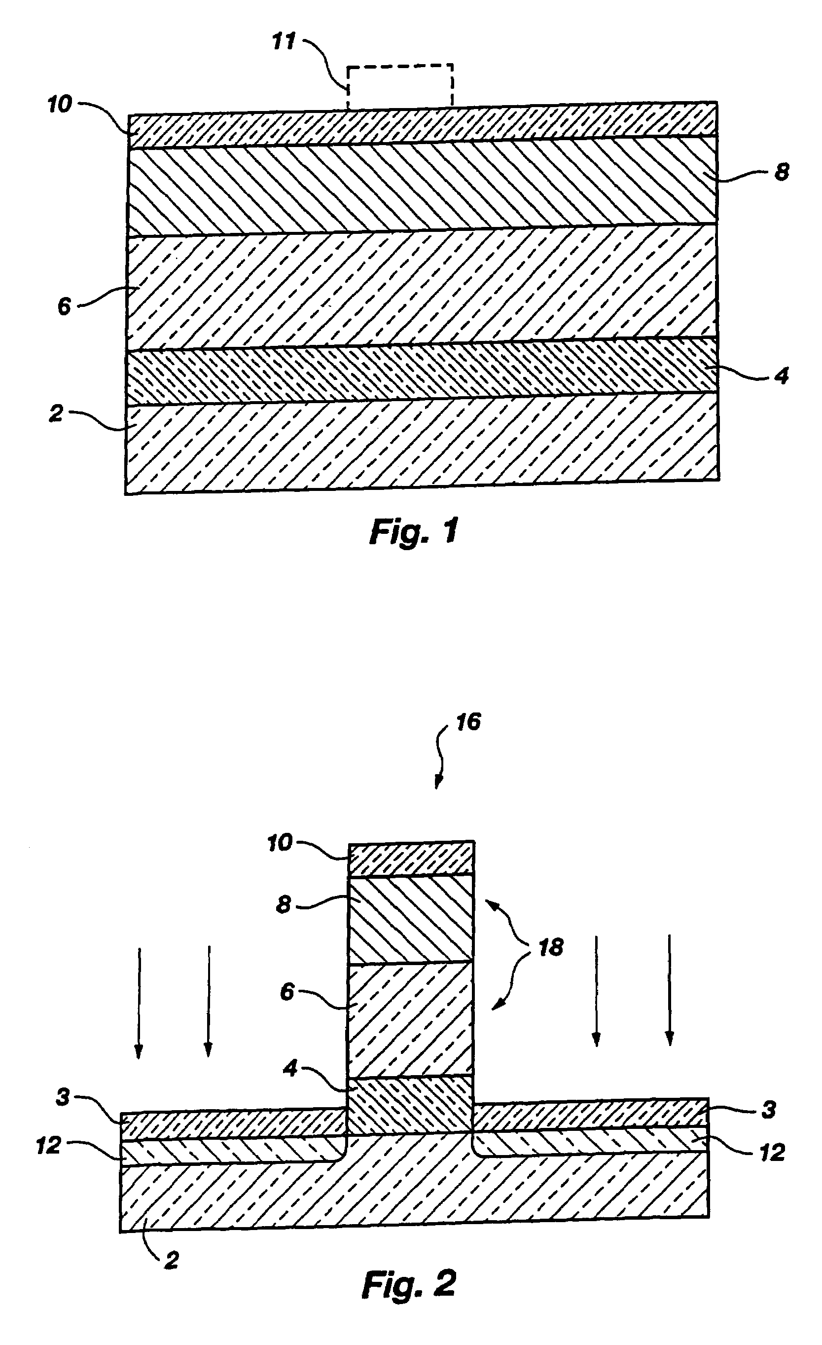
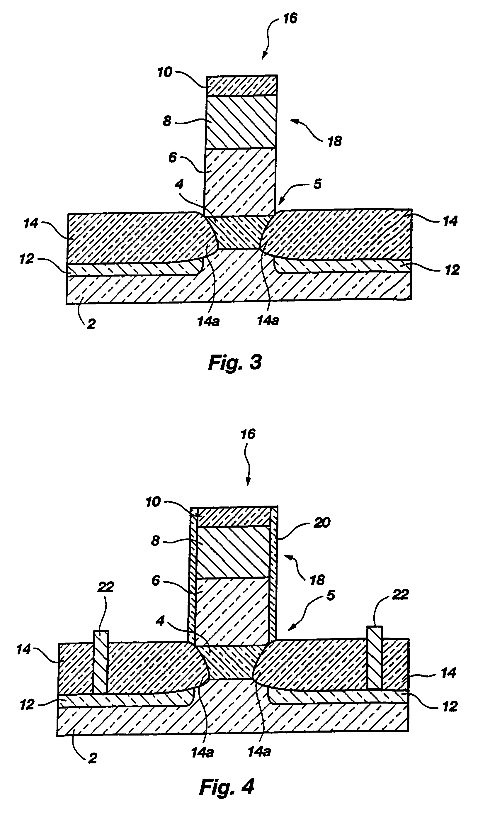
[0010]The present invention provides ion-assisted oxidation methods and the structures formed thereby. The ion-assisted oxidation methods are employed to form a high-quality oxide layer over source and drain regions of a substrate. The ion-assisted oxidation methods form this high-quality oxide layer when inert ions, such as argon, vertically bombard a pre-existing oxide layer on the substrate or structures thereof in an atmosphere containing at least one oxidant, thereby increasing the quality and thickness of the pre-existing oxide layer. The energy for forming the high-quality oxide layer comes from the energy of the inert ions, rather than a high temperature.

[0011]The following description provides specific details such as material thicknesses and types in order to provide a thorough understanding of the present invention. The skilled artisan, however, would understand that the present invention may be practiced without employing these specific details. Indeed, the present inven...


PUM

PropertyMeasurementUnit
temperatureaaaaaaaaaa
energyaaaaaaaaaa
thicknessaaaaaaaaaa

Abstract

Oxidation methods and resulting structures including providing an oxide layer on a substrate and then re-oxidizing the oxide layer by vertical ion bombardment of the oxide layer in an atmosphere containing at least one oxidant. The oxide layer may be provided over diffusion regions, such as source and drain regions, in a substrate. The oxide layer may overlie the substrate and is proximate a gate structure on the substrate. The at least one oxidant may be oxygen, water, ozone, or hydrogen peroxide, or a mixture thereof. These oxidation methods provide a low-temperature oxidation process, less oxidation of the sidewalls of conductive layers in the gate structure, and less current leakage to the substrate from the gate structure.

Description

CROSS-REFERENCE TO RELATED APPLICATIONS[0001]This application is a continuation of application Ser. No. 09 / 934,916, filed Aug. 22, 2001, now U.S. Pat. No. 6,770,538, issued Aug. 3, 2004, which is a continuation of application Ser. No. 09 / 146,710, filed Sep. 3, 1998, now U.S. Pat. No. 6,355,580, issued Mar. 12, 2002.BACKGROUND OF THE INVENTION[0002]This invention relates generally to the field of integrated circuit design and fabrication. Specifically, the invention relates to ion-assisted oxidation methods and the structures formed thereby.[0003]Silicon oxide is used in integrated circuit (IC) and semiconductor fabrication, especially metal-oxide-semiconductor (MOS) fabrication, due to its excellent dielectric properties for insulation and field enhancement. See, for example, U.S. Pat. Nos. 4,776,925 and 5,521,126, the disclosures of which are incorporated herein by reference. Silicon oxide, both doped and undoped, is especially useful for fabrication of transistors. A transistor is...

Claims


Application Information

Patent Timeline
Patent Type & Authority Patents(United States)
IPC IPC(8): H01L21/31H01L21/3105H01L21/265H01L21/314H01L21/316H01L21/336
CPCH01L21/02238H01L21/02255H01L21/02351H01L21/31662H01L21/76213H01L29/42368H01L29/66575H01L21/0223H01L21/28008H01L21/26506H01L21/823412Y10S148/116H01L21/823807Y10S148/118
Inventor LI, LIPAN, PAI-HUNG
Owner MICRON TECH INC
Why Eureka
Try Eureka