Field effect transistor and method for fabricating it

a field-effect transistor and field-effect technology, applied in the field of field-effect transistors, can solve the problems of increasing the difficulty of ensuring adequate forward current ions above a feature size of about 100 nm, increasing the packing density, and increasing the difficulty of conventional field-effect transistors, so as to achieve the effect of reducing or avoiding, low outlay

Inactive Publication Date: 2006-10-10
POLARIS INNOVATIONS LTD
View PDF14 Cites 31 Cited by
  • Summary
  • Abstract
  • Description
  • Claims
  • Application Information

AI Technical Summary

Benefits of technology

[0013]The present invention provides a field-effect transistor and a method for fabricating it which reduce or avoid the abovementioned difficulties. In particular, the present invention provides a field-effect transistor makes available an adequate forward current ION and which can be fabricated with a low outlay, compatibly with the previous conventional integration process for planar MOSFETs.
[0034]The field-effect transistor according to the invention has the advantage that a significant increase in the effective channel width for the forward current ION can be ensured compared with previously known, conventional transistor structures, without having to accept a reduction of the integration density that can be attained. In the case of the field-effect transistor according to the invention, the planar channel region at the upper surface of the elevation is extended in width by additional vertical channel regions at the side areas of the elevation. These additional vertical channel regions directly adjoin the planar channel region (vertical extended channel regions). Furthermore, the field-effect transistor according to the invention has a small reverse current IOFF. These advantages are obtained without having to reduce the thickness of the gate insulator into the region of the tunneling of charge carriers or reduced stability.
[0037]In accordance with one preferred embodiment of the field-effect transistor according to the invention, the second gate oxide layer is made thicker on the lateral surfaces of the first gate electrode than on the lateral surfaces of the web-type elevation. Furthermore, it is preferred if an insulating spacer is arranged on the second gate oxide layer at the level of the first gate electrode. This makes it possible to further reduce the electric field strength at the edges.
[0038]In accordance with a further preferred embodiment of the field-effect transistor according to the invention, the edges of the web-type elevation are rounded between the upper surface and the lateral surfaces. This rounding can preferably be produced with the aid of a short high-temperature process. Accordingly, the transistor according to the invention can be processed with a significantly reduced temperature budget. This yields advantages interalia in respect of doping profiles and performance. Moreover, as a result, the transition region between the planar and vertical channel regions is kept small, and virtually the entire width and depth of the geometrical channel area can be utilized as active channel even in the event of a very highly scaled transistor geometry.

Problems solved by technology

The characteristic parameters of conventional field-effect transistors, in particular of planar MIS field-effect transistors (MISFET), are increasingly impaired with continual structural miniaturization (scaling) and increasing of the packing density of integrated circuits.
Despite all these measures, however, it is becoming more and more difficult to ensure adequate forward currents ION above a feature size of about 100 nm, without the risk of tunneling or degradation of the gate oxide stability of the MISFET.
Unfortunately, all of the measures mentioned either have only limited efficacy or they require a high process engineering outlay.

Method used


Image

  • Field effect transistor and method for fabricating it
  • Field effect transistor and method for fabricating it
  • Field effect transistor and method for fabricating it

Examples


Embodiment Construction

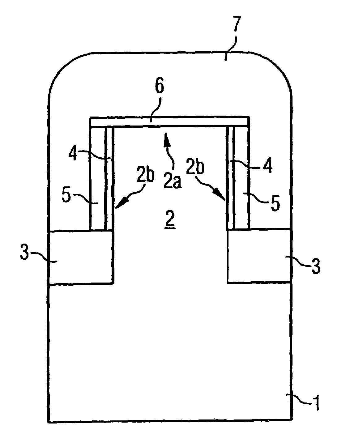
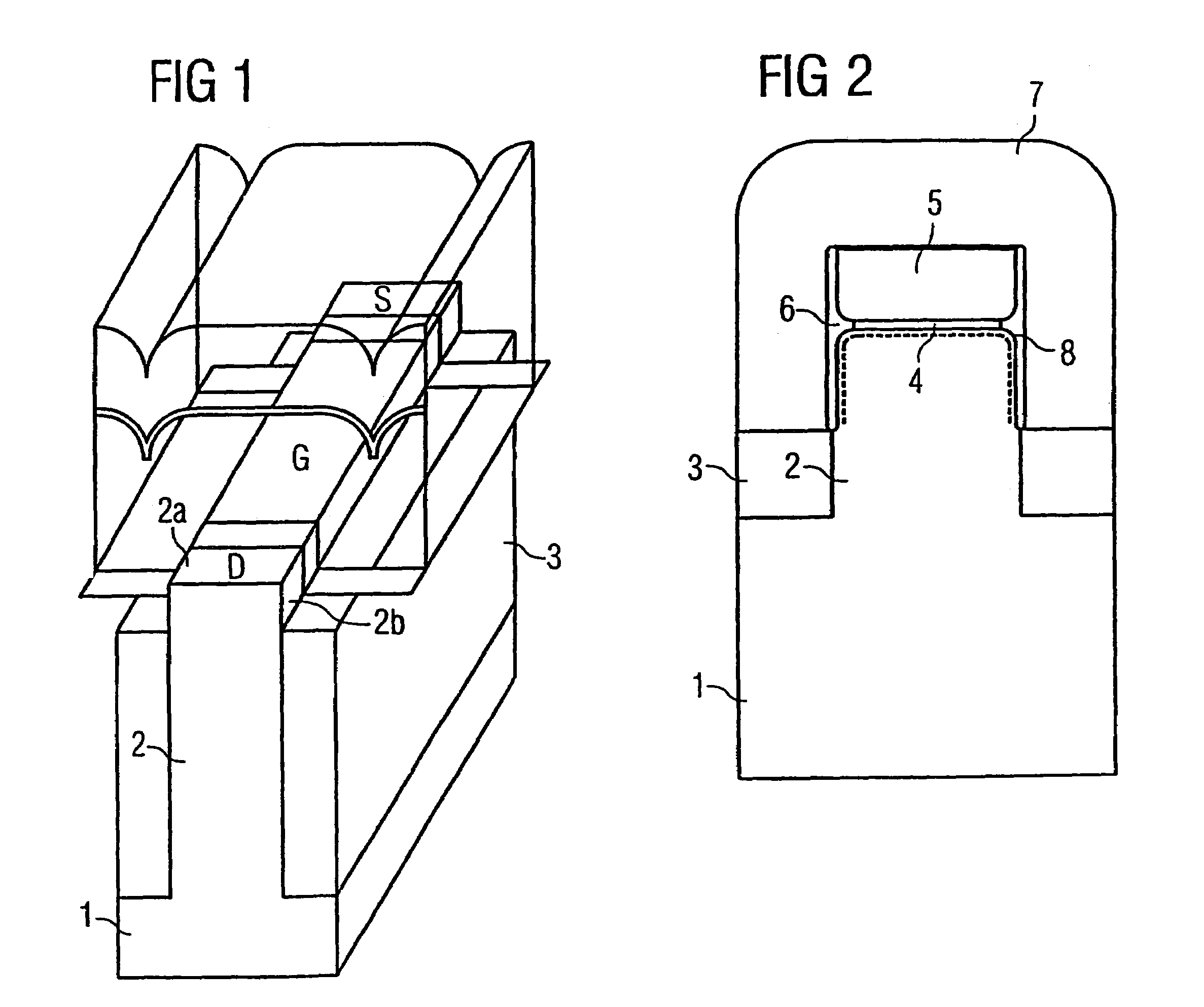
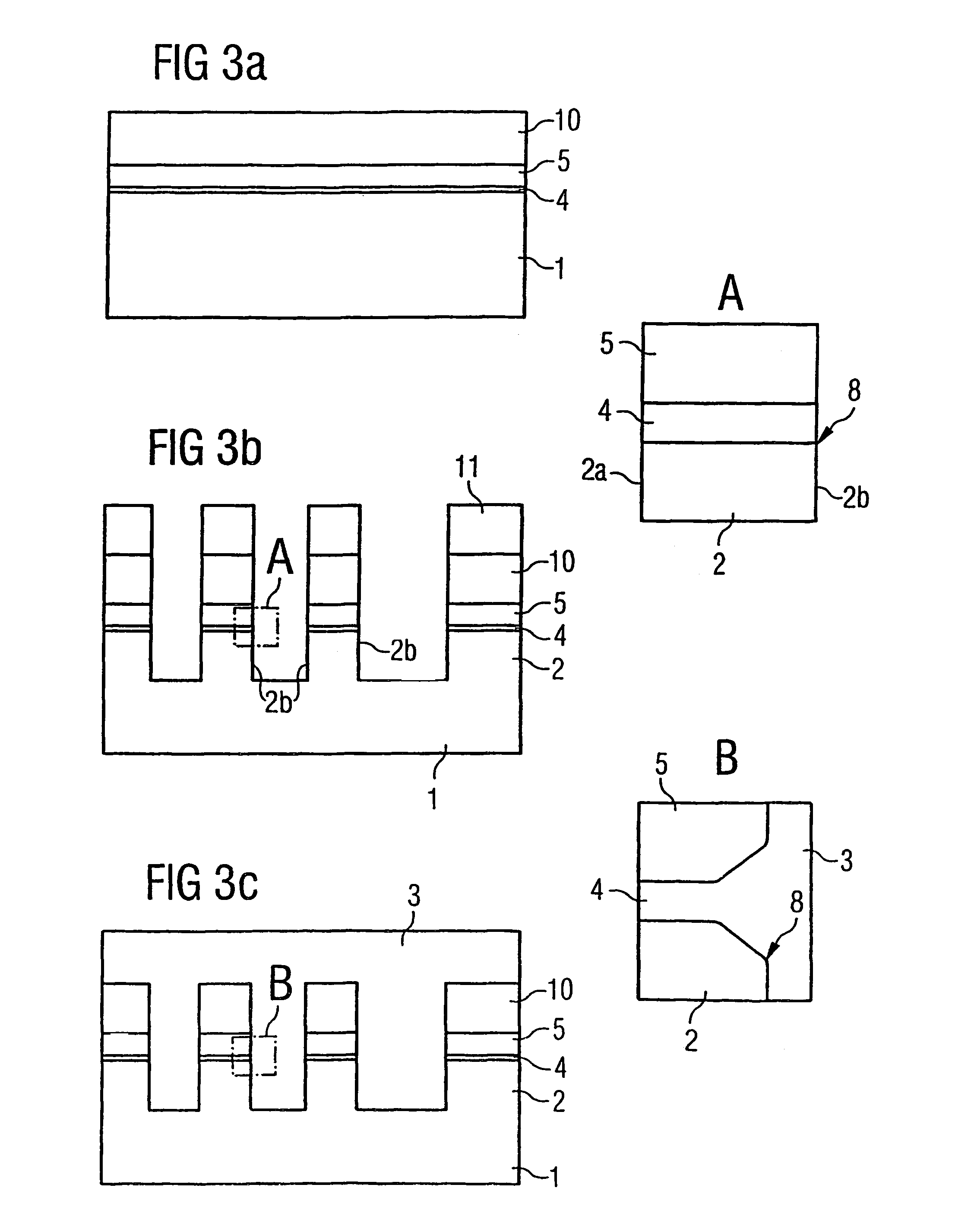
[0050]FIGS. 1 and 2 show a first embodiment of the field-effect transistor according to the invention. In this case, FIG. 1 shows the general structure of this embodiment of the field-effect transistor according to the invention, while FIG. 2 illustrates the details of this according be seen according which is embodiment of the field-effect transistor to the invention in a cross section. As can from FIG. 1, the field-effect transistor to the invention has a web-type elevation 2, arranged on a semiconductor substrate 1 and has an upper surface 2a and two lateral surfaces 2b. The web-type elevation 2 constitutes the active semiconductor region in this case.

[0051]The active semiconductor region 2 with vertical connection to the semiconductor substrate 1 is laterally insulated from adjacent active regions (not illustrated) by STI field isolation regions 3. The surface 2a, 2b of the active region is patterned into source and drain regions and also into a planar channel region. The web-ty...


PUM


Abstract

The invention relates to a field effect transistor in which the planar channel region on the upper surface of the elevation is extended in width by means of additional vertical channel regions on the lateral surfaces of the elevation. Said additional vertical channel regions connect directly to the planar channel region (vertical extended channel regions). Said field effect transistor has the advantage that a significant increase in the effective channel width for the current flow ION can be guaranteed relative to conventional transistor structures used up until the present, without having to accept a reduction in the achievable integration density. Said field effect transistor furthermore has a low reverse current IOFF. The above advantages are achieved without the thickness of the gate insulators up to the region of the charge transfer tunnels having to be reduced or a reduced stability.

Description

CLAIM FOR PRIORITY[0001]This application is a national stage of PCT / EP02 / 07028, filed in the German language on Jun. 25, 2002, and which claims the benefit of priority to German Application No. DE 101 31276.8, filed in the German language on Jun. 28, 2001.TECHNICAL FIELD OF THE INVENTION[0002]The present invention relates to a field-effect transistor and a method for fabricating it.BACKGROUND OF THE INVENTION[0003]The characteristic parameters of conventional field-effect transistors, in particular of planar MIS field-effect transistors (MISFET), are increasingly impaired with continual structural miniaturization (scaling) and increasing of the packing density of integrated circuits. Thus, by way of example, with a shortened channel length of the transistor the threshold voltage VT of the transistor decreases. At the same time, with a shortened channel length, the field strength in the channel region and the reverse current IOFF increase (SCE: short channel effect; roll-off). Furthe...

Claims


Application Information

Patent Timeline
Patent Type & Authority Patents(United States)
IPC IPC(8): H01L29/76H01L29/94H01L31/062H01L31/113H01L31/119H01L29/423H01L21/336H01L29/49H01L29/78H01L29/786
CPCH01L29/66484H01L29/66795H01L29/7831H01L29/7851H01L29/7854H01L29/78
Inventor POPP, MARTINRICHTER, FRANKTEMMLER, DIETMARWICH-GLASEN, ANDREAS
Owner POLARIS INNOVATIONS LTD
Why Eureka
Try Eureka